Quantcast
Channel: Other Projects - PIC Microcontroller
Viewing all 223 articles
Browse latest View live

Mädchen Machen Technik

$
0
0

The “Mädchen Machen Technik” workshop is designed to give high school students an introduction to microcontrollers. The students will build a flashing light pattern and/or a counter-timer. In the process of building this project, the students will learn about microcontrollers and digital electronics. Here is the parts list for the projects.

Introduction to some circuit elements

  1. The students will learn how to measure DC voltage and resistance using a multi-meter. They will measure the voltage of batteries connected in series and in parallel.
  2. The students are given the task to determine, using a voltmeter and wires, how the holes on a breadboard are connected. The students sketch the hole connections on a picture of the breadboard.
  3. Next, the students will be given several Light Emitting Diodes (LEDs), with an explanation on how they work. They are to connect the LED(s) to the breadboard so that one LED lights up, then two light up, etc. Do not put more than 3 Volts across an LED.

Blinking Lights ProjectAs a first project on the breadboard, we will program the microcontroller to produce a blinking pattern of up to five LED’s. We will start with one of the simplest microcontrollers: PIC12F629. First, we build the circuit on the breadboard, then we will program the PIC12F629 chip.

Building the Circuit

  1. A schematic of the circuit is shown below:
  2. The PIC12F629 has only 8 pins. Pin 8 is the ground pin, and Pin 1 is the positive voltage pin. In our applications, we will use two AA batteries in series which will give around 3 volts for Pin 1.
  3. The other six pins (2-7) will be used as digital input/output. Pins 2, 3, 5, 6, and 7 will be output pins connected to LEDs. Pin 4 can only be set as an input pin. We will not connect an LED to pin 4. In the picture below, one can see the 5 LEDs connected to the appropriate pins.Mädchen Machen Technik

Building the ProgrammerAfter setting up the “blinking lights project” on the breadboard, we program the chip. To program the microcontroller, we will need to constuct a programmer circuit on a bread board. Each group of three students will use the same programmer, a pickit2. The programmer circuit is shown below

PicP1

The programmer has 6 pins in a row. The ground on the programmer, pin 3, is connected to the ground of the chip (pin 8). The voltage (5V) of the programmer, pin 2, is connected to pin 1 of the chip. The other programmer pins are connected to the chip.

The pickit2 is connected to a personal computer through a usb port. In the picture below, one can see where the microcontroller chip is connected in the programmer:

Finally, we program the microcontroller using the MPlab software from microchip.

Programming the Microcontroller

  1. The assembly code we will start with is the code: test12.asm. The only lines of the code the students need to modify for their desired blinking pattern are:loop
    movlw b’00100101′
    movwf GPIO
    call delay1
    movlw b’00010010′
    movwf GPIO
    call delay1
    goto loop

    First, the binary number ‘00100101’ is placed in the working register. Then this number in the working register is transfered into the register GPIO. The GPIO register is directly connected to the pins of the chip. A “1” will put 3 volts on a pin, and a “0” will put zero volts on the pin. The last 6 bits are connected to pins 2, 3, 4, 5, 6, and 7 respecively. The number ‘00100101’ in register GPIO will result in 3 volts for pins 2, 5, and 7, and zero volts for pins 3 and 6. Pin 4 is not affected, it is only an input pin. The subroutine delay1 causes a delay of around 1/4 second.

    Then, the binary number ‘00010010’ is placed in the working register and then transfered to the GPIO register. The number ‘00010010’ will produce 3 volts on pins 3 and 6, and zero volts for pins 2, 5, and 7. After a delay of 1/4 second, the chip goes back to “loop” and repeats the pattern.

  2. The students can program any pattern of the five LED lights by modifying the lines in the loop.

Read More:   Mädchen Machen Technik

The post Mädchen Machen Technik appeared first on PIC Microcontroller.


Temperature controlled fan using PIC 16F877A

$
0
0

You might have come across several applications where we need to control a specific device based on analog parameter. This Embedded system works in a similar concept where we are about to control the speed of a DC motor using based on the external temperature. The rise in temperature will result in increase in speed of the motor and vice versa. These type of Temperature controlled fan systems can generally be used to maintain temperature of a room or object automatically.

temperature-controlled-dc-motor-pic16f877a

 DESIGN OF TEMPERATURE CONTROLLED FAN SYSTEM:

  • The temperature is measured by means of a temperature sensor LM35.
  • The output voltage of the sensor is fed to the A/D channel of the Microcontroller.
  • Based on the sensed temperature the speed of the motor is controlled using PWM .
  • Several temperature ranges was set in the code to vary the motor speed based on the level of temperature sensed.
  • The speed of the motor is controlled by using PWM.
  • The motor is driven using a driver IC l293D, See a brief explanation on its working and wiring here.

LM35:

Lm 35 is used to sense the external temperature which is capable of sensing temperature ranges from -55 to 150 C. The output voltage is proportional to the temperature hence there is no need of trimmers to calibrate the reading. The output voltage of this sensor varies by 10mv per degree change in temperature.

CALIBRATION:

We are using a 10 bit ADC and Vcc as Vref to the ADC module of the Controller. So in order to determine the step size we have to divide the Vref by our resolution that is 2^10 ( 1024 ).

Step Size = 5 / 1024 = 4.83mV

We obtain a change of 10mV with each rise or fall in temperature from the sensor. And value in the ADC register will alter by two steps with each degree change in the sensor since two increments of step size i.e 4.833mV * 2 = 9.96mV which is approximately equal to 10mV. So in order to obtain the original value we have to divide the contents in the ADC register by 2

Real value = ADC value / 2


Read More:   Temperature controlled fan using PIC 16F877A

The post Temperature controlled fan using PIC 16F877A appeared first on PIC Microcontroller.

Digital Count Down Timer using PIC Microcontroller

$
0
0

In this article, our author Mithun has developed a 0 – 99 min counter using PIC microcontroller 16F628A. So basically this is a digital count down timer ideal for engineering and diploma students for their project requirements. We have given complete circuit diagram of the digital count down timer along with full source code. In addition, photographs of the breadboard setup is uploaded.

diagram1

Every micro controller has a timer unit inside. A timer is nothing more than a time counting device fabricated inside the micro controller unit. A wide range of practical applications require a timer in action. For example, we need to turn a motor ON for 5 minutes and then turn it OFF as part of a particular project; how will we do that? A timer inside a mircocontroller unit aids us in implementing this perfectly. A timer can be used to count the 5 minutes exactly and the bits that get SET at 5 minutes limit can be used to program the controller to turn OFF some device(s).

I hope you got a basic idea about timer unit and its practical applications. We are going to make this project using an LCD display, PIC controller 16F628A and a 4 MHz external crystal to provide the necessary clock. We will be writing the codes using micro C.

In any project that involves an LCD, the first step is to initialize the LCD module. We have written detailed articles about interfacing LCD to an MCU before. You can learn more about Interfacing an LCD to 8051  and Interfacing LCD module to AVR controller in these articles. If you want to learn more about character LCD displays in detail, this tutorial on Character LC

D displays will be of help.

11

Now, we need to configure relay and switches. The code snippet for the same is given below.

002


Here ‘sbit’ stands for set bit. You can do the same another way using “#define” command. This line means that  RA3 pin will be known as the Relay/ RB0 pin will be known as SS_Select etc.

Even though the project name “digital count down timer” sounds so silly, its operation is not that simple. We have given below a proteus diagram of the circuit to explain the project perfectly.

Analyzing the circuit diagram, you can see three buttons . One button is for Start/Stop function and the other 2 buttons for Units & Tens counting. We will configure our LCD module with display messages corresponding to the button configurations.


Read More:   Digital Count Down Timer using PIC Microcontroller

The post Digital Count Down Timer using PIC Microcontroller appeared first on PIC Microcontroller.

Interfacing Bluetooth Module HC-06 with PIC Microcontroller

$
0
0

In this tutorial we will learn How to make out PIC projects wireless by interfacing a Bluetooth Module (HC-06). In our previous tutorial we have already learnt How to use USART module in our PIC Microcontroller and established communication between PIC and Computer. If you are an absolute beginner then check here for our all the PIC Tutorials, where we have started from the scratch, like learning MPLAB and XC8, interfacing LED, LCD, using Timers, ADC, PWM etc.

Interfacing Bluetooth Module HC-06 with PIC Microcontroller

Here, we have used the popular Bluetooth module HC-06. Using this module we can receive and send information wirelessly from our PIC MCU to a mobile application or a computer. Communication between PIC and HC-06 is established using the USART module present in the PIC Microcontroller. You can also use the HC-05. We again operate on the same Asynchronous 8-bit mode, but this time we will modify our code a bit so that it works with the Bluetooth module. Hence learning UART tutorial beforehand is an added advantage for this project.

In this tutorial, we will toggle a LED by sending on or off command from our Smart phone. We will use an Android application called Bluetooth Terminal which can send and receive data over Bluetooth. If we send a char ‘1’ from the app the light will be turned ON in the PIC board and we will get an acknowledgment back to the phone that the light has been turned on. Similarly we can send ‘0’ from phone to turn it off. This way we can control the LED light on our PIC board, similar to the UART tutorial but now wirelessly. Complete Program and the Detailed Video is given at the end of this tutorial.

The basic block diagram for the setup is shown below.

Interfacing-Bluetooth-HC06-with-PIC-Microcontroller-block

Requirements:

Hardware:

  • PIC16F877A Perf Board
  • HC-05 or HC-06 Bluetooth Module
  • Computer (for programming )
  • Mobile Phone
  • PICkit 3 Programmer

Software:

Bluetooth Module HC-06:

Bluetooth can operate in the following two modes:

  1. Command Mode
  2. Operating Mode

In Command Mode we will be able to configure the Bluetooth properties like the name of the Bluetooth signal, its password, the operating baud rate etc. The Operating Mode is the one in which we will be able to send and receive data between the PIC Microcontroller and the Bluetooth module. Hence in this tutorial we will be toying only with the Operating Mode. The Command mode will be left to the default settings. The Device name will be HC-05 (I am using HC-06) and the password will be 0000 or 1234 and most importantly the default baud rate for all Bluetooth modules will be 9600.

Read More:   Interfacing Bluetooth Module HC-06 with PIC Microcontroller

The post Interfacing Bluetooth Module HC-06 with PIC Microcontroller appeared first on PIC Microcontroller.

UART Communication using PIC Microcontroller

$
0
0

In this tutorial we learn to Enable UART communication with PIC Microcontroller and how to transfer data to and from your Computer. So far, we have covered all basic modules like ADC, Timers, PWM and also have learnt how to interface LCDs and 7-Segment displays.  Now, we will equip our self with a new communication tool called UART which widely used in most of the Microcontroller projects. Check here our complete PIC Microcontroller Tutorials using MPLAB and XC8.

UART Communication using PIC Microcontroller

Here we have used PIC16F877A MCU, it has a module called “Addressable Universal Synchronous Asynchronous Receiver and Transmitter” shortly known as USART.  USART is a two wire communication system in which the data flow serially. USART is also a full-duplex communication, means you can send and receive data at the same time which can be used to communicate with peripheral devices, such as CRT terminals and personal computers.

The USART can be configured in the following modes:

  • Asynchronous (full-duplex)
  • Synchronous – Master (half-duplex)
  • Synchronous – Slave (half-duplex)

There are also two different modes namely the 8-bit and 9-bit mode, in this tutorial we will configure the USART module to work in Asynchronous mode with 8-bit communication system, since it is the most used type of communication. As it is asynchronous it doesn’t need to send clock signal along with the data signals. UART uses two data lines for sending (Tx) and receiving (Rx) data. The ground of both devices should also be made common. This type of communication does not share a common clock hence a common ground is very important for the system to work.

UART-Communication-using-PIC-Microcontroller-PIC16F877A

At the end of this tutorial you will be able establish a communication (UART) between your computer and your PIC Microcontroller and toggle an LED on the PIC board from your laptop. The status of the LED will be sent to your laptop from the PIC MCU. We will test the output using Hyper Terminal in computer. Detailed Video is also given at the end of this tutorial.

Requirements:

Hardware:

  • PIC16F877A Perf Board
  • RS232 to USB converter Module
  • Computer
  • PICkit 3 Programmer

Software:

  • MPLABX
  • HyperTerminal

A RS232 to USB converter is required to convert the serial data into computer readable form. There are ways to design your own circuit instead of buying your own module but they are not reliable as they are subjected noise. The one which we are using is shown below

RS232-to-USB-converter-Module

Note: Each RS232 to USB converter would require a special driver to be installed; most of them should get installed automatically as soon as you plug in the device. But, if it doesn’t relax!!! Use the comment section and I will help you out.

Programming PIC Microcontroller for UART Communication:

Like all modules (ADC, Timer, PWM) we should also initialize our USART module of our PIC16F877A MCU and instruct it to work in UART 8-bit communication mode.  Let’s define the configuration bits and start with the UART initialization function.

Initializing the UART module of the PIC Microcontroller:

The Tx and Rx pins are physically present at the pins RC6 and RC7. According to datasheet let’s declare TX as output and RX as input.

Read More:   UART Communication using PIC Microcontroller

The post UART Communication using PIC Microcontroller appeared first on PIC Microcontroller.

Dspic-Servo Project using PIC30F4012 microcontroller

$
0
0

Project Description

This project was developed as an inexpensive way to drive small dc brushed motors as positioning servos for use on a desktop sized CNC machine. The board is interfaced to the PC through 2 pins of a parallel port. The drive signal on these pins is known as quadrature drive.

Dspic-Servo

The power stage consists of a power op amp driven in constant current mode. The internal PIC processor ( a 30f4012 from Microchip ) is programmed in C through the C30 compiler and the Microchip IDE. The servo loop parameters are programmed through a serial port connection and are saved in the dspic eeprom. Once set for a particular drive, they should not need to be changed.
A YouTube video by Ted Maczulat.

The serial programming interface is used to tune the PID and other servo loop parameters to optimize the performance in a particular application. The serial port runs at a fixed baud rate of 9600N81. Any terminal program such as minicom, gtkterm, or hyperterminal may be used to talk to the dspic-servo. On powerup you will see the following:

Powerup...i/o...uart...timer...pwm...pid...encoder...capture...done

dspic-servo by L. Glaister
(c)25-Sept-2006 by VE7IT

using setup from eeprom.. ? for help

Current Settings:
servo enabled = 1
(p) = 0.020000
(i) = 0.000000
(d) = 0.000050
FF(0) = 0.000000
FF(1) = 0.000000
dead(b)and = 1.000000
(m)ax output = 2.500000
(f)ault error = 1024.000000
(x)pc cmd multiplier = 3
(t)icks per servo cycle= 10

To change a value, type the cmd letter/number and then a value for example:

p0.03

The current values will be redisplayed with the new value set. The p,i,d, ff0 and ff1 values are standard loop gain parameters. You can reference the source code for a better explanation. The deadband parameter is the number of encoder counts the servo can be out of position without the servo loop taking any corrective action. The max output is the maximum current output allowed in amps and should be set for the particular motor you are using. This number can be up to 7 amps. The fault error parameter is used to set the number of counts the servo can be out of position before the drive gives up and indicates a drive fault. This is used to detect crashes and jammed axis or input command conditions beyound the capabilities of the motor. The pc command multiplier is useful for cases where you have a high resolution encoder on the motor and a PC that is limited in the number of pulses/second it can output. For most operation this number will be set to 1, but if you have trouble reaching the top speed you need from the drive, it may be helpful to set this number to a higher value. The internal servo loop works by keeping 2 counters. The first is the commanded position from the PC, the second is the actual position from the encoder. The servo loop of the drive attempts to keep these 2 numbers as close as possible to each other.


For more detail: Dspic-Servo Project using PIC30F4012 microcontroller

The post Dspic-Servo Project using PIC30F4012 microcontroller appeared first on PIC Microcontroller.

Schematic PIC Data Logger with Delta-Sigma Converter

$
0
0
The aim of the project is to build a lab-grade data logger with PIC18F45K20 microcontroller and a 20-bit delta-sigma converter. It’s named as G5 Data Logger.

This new data converter technology using delta-sigma simplifies the design of high resolution data recording device. One of the interesting chip is Linear Technology LTC2400, 24-bit ADC. Another chip of interest is LTC2420, 20-bit ADC.

 Schematic PIC Data Logger with Delta-Sigma Converter
The chip has pin and data output compatible to the LTC2400. This project uses new data logger using the LTC2420 and use the cheap memory card for data storage.

DownloadSchematic, Firmware, Quick start, Brochure, Sample record of TMP36

The post Schematic PIC Data Logger with Delta-Sigma Converter appeared first on PIC Microcontroller.

Interfacing Relay with PIC Microcontroller

$
0
0

A relay is an electromagnetic switch which is used to switch High Voltage/Current using Low power circuits. Relay isolates low power circuits from high power circuits. It is activated by energizing a coil wounded on a soft iron core. For detailed working of relay please visit this page. A relay should not be directly connected to a microcontroller, it needs a driving circuit.

A relay should not be connected directly to a microcontroller due to following reasons..

  • A microcontroller is not able to supply current required for the working of a relay. The maximum current that a PIC Microcontroller can source or sink is 25mA while a relay needs about 50 – 100mA current.
  • A relay is activated by energizing its coil. Microcontroller may stop working by the negative voltages produced in the relay due to its back emf.Interfacing Relay with PIC Microcontroller

    Interfacing Relay with PIC Microcontroller using Transistor

    A relay can be easily interfaced with microcontroller using a transistor as shown below. Transistor is wired as a switch which carries the current required for operation of the relay. When the pin RB7 of the PIC microcontroller goes high, the transistor BC547 turns On and current flows through the relay.  The diode D1 is used to protect transistor and the microcontroller from Back EMF generated in the relays coil.  Normally 1N4148 is preferred as it is a fast switching diode having a peak forward current of 450mA. This diode is also known as freewheeling diode.

    Schematic Interfacing Relay with PIC Microcontroller

    Interfacing Relay with PIC using Transistor

Note: VDD and VSS of the pic microcontroller is not shown in the circuit diagram. VDD should be connected to +5V and VSS to GND.

Read More: Interfacing Relay with PIC Microcontroller

The post Interfacing Relay with PIC Microcontroller appeared first on PIC Microcontroller.


Making a simple clap switch

$
0
0

A clap switch is a fun project for beginners. It switches on and off electrical appliances with a sound of clapping hands. Today we will discuss about making a simple clap switch that operates when it detects two clapping sounds in a row. It uses an electret microphone as a transducer for converting a clapping sound into an electrical signal. The microcphone output is amplified by a transistor and is then sent to the PIC12F683 microcontroller which performs an ON/OFF switching action when valid claps are detected.

Making a simple clap switch

Simple clap switch using a condenser mic and PIC microcontroller

Theory

The clap switch requires a transducer at the input to convert sound vibrations from clapping hands into electrical energy. An electret microphone or simply mic (OBO-04FN-0B) is used for this purpose. The output from the mic is very low in magnitide and so we need an amplifier circuit to boost the detected sound signal. The following circuit diagram shows the mic along with a single transistor amplifier. When there’s no sound, the collector voltage (Vout) of the transistor, which is saturated, is approximately 0.2V. When the mic detects a clap sound, the voltage across it drops suddenly. Since the condenser mic’s output voltage is coupled to the base of the transistor through capacitor C1, the base-emitter voltage is also lowered and as such the base-emitter junction is less forward biased or cutoff (in case of high clap sound). Therefore, every time a clapping sound is detected, there is a sudden peak arising at the collector voltage.

Schematic Making a simple clap switch

Sensor part

The following picture shows the peaks in the collector voltage due to multiple clap sounds. You can see the peak voltage can go as high as 4.0V depending on the loudness of the clap. This waveform of the collector voltage is captured using Digilent’s Analog Discovery device.

For more detail: Making a simple clap switch

The post Making a simple clap switch appeared first on PIC Microcontroller.

Digital logic probe for troubleshooting TTL and CMOS circuits

$
0
0

A logic probe is considered as a stethoscope for engineers and technicians for debugging digital logic circuits that consists of logic gates, memories, registers, etc. A digital multimeter (DVM) can also be used for such analytical purposes but it gives you the numeric value of the voltage at a point instead of the logic state. Depending on whether the circuit is based on TTL or CMOS components, the voltage levels for logic 0 and 1 could be different for each family. DVM users, thus, have to calculate logic levels from the measured voltages, which consumes time and delays the troubleshooting procedure. A logic probe, on the other hand, does all these functions automatically and shows meaningful logic states at test points. In this project, we will discuss about making a digital logic probe that is applicable to both TTL and CMOS circuits and uses minimal components.

Digital logic probe for troubleshooting TTL and CMOS circuits

Logic probe for CMOS and TTL circuits

Theory

There are mainly two logic families used in digital circuits: TTL and CMOS. While TTL operates at +5V, the power supply for CMOS circuits could range from +3V to 15V. According to the standard TTL convention, any voltage less than 0.8V is defined as logic low while any voltage above 2.2 is defined as logic high and anything in between these extremes is defined as intermediate state. In case of CMOS circuits, any voltage less than 1/3 of VDD is defined as logic low while any voltage above 2/3 of VDD is defined as logic high. Any voltage between these values is defined as intermediate or transitional state. This logic probe works for both TTL and CMOS circuits powered from +5V to 15V.

This logic probe consists of a 78L05 voltage regulator, a Microchip PIC12F683 microcontroller, a CD4094BE CMOS shift register and a tiny seven segment display. Since the operating voltage range of this logic probe is between 5 to 15V, the role of the 78L05 voltage regulator is to ensure that the microcontroller and the rest of the circuit are always powered with a stable 5V source. There are two voltage divider networks, each made from a 9.1K  and a 1K Ohms (1% tolerance) resistors. The outputs of the two networks go to the ADC channels AN0 and AN1. The AN0 channel reads the logic level voltage of the test pin whereas the AN1 channel is used to measure the supply voltage of the test circuit. The information of the supply voltage is necessary to identify a CMOS circuit powered with > 5V. The GP2, GP4, and GP5 pins of PIC12F683 drives the CD4094 shift register. The shift register acts as an I/O expander in this application and its outputs are connected to a seven segment display.

Schematic Digital logic probe for troubleshooting TTL and CMOS circuits

Circuit diagram of the logic probe (click on image to enlarge)

Software

The software for this project is written in MikroC PRO for PIC version 5.30. Only the ADC built-in library is used. The rest of the code is written without any library aid. The code starts with the definitions of pin names and common variable declarations. Apart from the main function which does all the tasks, there are six functions in the code. The setup() function sets directions of I/O pins and initiates the built-in ADC for data acquisition. The test_display() function tests the LEDs of the seven segment display connected to the shift register. The way this is done with the shift register will be discussed later in this text. The feature that makes this logic probe universal and unique is its ability to determine the supply voltage level. In the function test_supply(), the power source is tested. During this test if it is found that the ADC average of supply voltage is within the span of 4.75V to 5.25V then the standard TTL minimum high and maximum low logic level voltages are set, otherwise conventional CMOS logic level voltage values are set. These values are kept in the variables called high_level and low_level and are retained till power down. The display(unsigned char val) function is a software-hardware link between the shift register and the micro. It converts any 8 bit value given to the variable val in a way that it can be sent as an output just like a regular I/O port. The strobe pin is at first kept low to allow the access of the internal latches of the CD4094. Eight clock pulses are needed to shift data into the latches. During each clock pulse to the shift register, the variable val’s most significant bit (MSB) is read first and is sent as a data to the data input of the shift register. After sending data to the data pin, val is left shifted once and the clock pin is also toggled once. At the end of eight cycles the strobe pin is pulled high and the display is updated. The adc_avg(unsigned char ch) function read the designated ADC channel by taking 16 samples of ADC data and converting these samples into an average voltage value. Lastly the check_logic() function checks the logic input and sends logic symbol data to the seven segment display.

For more detail: Digital logic probe for troubleshooting TTL and CMOS circuits

The post Digital logic probe for troubleshooting TTL and CMOS circuits appeared first on PIC Microcontroller.

Business Card PIC Programmer using PIC12F629 microcontroller

$
0
0

Business Card PIC Programmer

Business Card PIC Programmer

This was my entry for the Hack A Day business card size circuit contest. I just zipped up the files and put them on my website. I’m posting it here because all the other entries seem to be on a blog for easy access. Hopefully this will make the project more accessible and reduce the load on my server.

The attached archive is the contest entry as it was on my server, minus the images. The text is taken from the included document.
This PIC/EEPROM programmer is so simple and small it fits on a business card with enough room left for assembly instructions…

Project:
Simple JDM2 style PIC ICSP programmer (on a business card).

  • all through hole
  • less than 2USD worth of parts (in 1s and 2s!)
  • easy single sided construction at home (with 3 jumpers)
  • enough room left for assembly instructions
  • extra space on the back for even more business-cardy goodness
  • also programs/reads serial EEPROMS

Skill level:
Easy/beginner.

Assembly time:
About an hour.

Step 1

Description

Anyone can build this simple programmer and learn about PIC microcontrollers. The JDM2 programmer is super simple (about 10 parts), but programs a huge variety of PICS and serial EEPROMs. I’ve programmed everything from an 8 pin 12F629 to a new 18F4550 USB PIC with the JDM2. This programmer has an ICSP interface, meaning it can program PICs and read EEPROMs while they are attached to a circuit board. Start your hacking!

The PCB can be made single sided (with three jumper wires), but a two layer design makes assembly even easier. All the traces are nice and fat for easy toner-transfer or photo-process at home.

The JDM2 design is quite old, the original JDM2 circuit can be found here:

http://www.jdm.homepage.dk/newpic.htm

This design stays true to the old schematic, but the diode numbering now starts at 1, rather than 2.

Step 2

Parts

Part Value Description

Schematic  Business Card PIC Programmer

C1 100uF/16 volt electrolytic capacitor
C2 22uF/16 volt tantalum capacitor
D1 8.2V zener diode
D2 5.1V zener diode
D3,4,5,6 1N4148 diode
Q1,2 BC547B transistor-npn
R1 10K resistor
R2 1.5K resistor
SV1 5 pin header pin header (or female pin header, you choose)
X1 DB9 female serial connector

Step 3

Assembly #1

Start from the bottom and work up:
Don’t forget to begin with the jumper wires if you are using a single sided PCB.
  • Solder the diodes and resistors.
  • Each diode has a black band that should be oriented in the same direction shown on the board/in the schematic.
  • Just solder in the resistors, no special orientation required.

Step 4

Assembly #2

Next, add the transistors. They should be oriented at show in the schematic/picture. The transistor on the left is placed in the direction opposite the transistor on the right (notice both have round parts facing the middle). This is the standard (typical?) BC547B pin-out. If you have problems with your finished circuit, make sure that your transistors have the same pin-out as shown in the schematic and reorient as needed.

The post Business Card PIC Programmer using PIC12F629 microcontroller appeared first on PIC Microcontroller.

Interfacing the Microchip PIC18F Microcontroller Master Synchronous Serial Port (MSSP) to various I2C Devices

$
0
0

The Inter-Integrated Circuit or I2C (read as I square C) bus has been introduced in 1980 by Philips, and has become a de-facto world standard for data exchange between Microcontroller and various devices such as temperature sensor, ADC (analog to digital converter), DAC (digital to analog converter), I/O expander, EEPROM, and many more. With more than thousand different IC devices have been manufactured with an I2C-bus interface, making the understanding of the working principle of this I2C bus is an essential knowledge that has to be acquired by anyone who want to involve in the embedded world professionally or just as hobbyist.

In this project we will learn of how to use the powerful 8-Bit Microchip PIC18F14K22 microcontroller Master Synchronous Serial Port (MSSP) in the I2C master mode to control various I2C devices simultaneously

Interfacing the Microchip PIC18F Microcontroller Master Synchronous Serial Port (MSSP) to various I2C Devices

The I2C Bus Protocol

The I2C bus use master and slave communication principle which mean the slave will response to any master request and only one master or one slave could use the I2C bus at the time (half-duplex communication). Therefore the master and slave have to be connected known as “Wired OR” connection using the pull-up resistors for both the I2C serial data (SDA) and serial clock (SCL) as shown on this following picture.Schematic Interfacing the Microchip PIC18F Microcontroller Master Synchronous Serial Port (MSSP) to various I2C Devices

Unlike the SPI (Serial Peripheral Interface) slave devices, the I2C devices don’t have the chip select (CS) pin where the SPI master could simply drive the CS pin to logic “0” in order to communicate with the target SPI slave device, instead in I2C protocol the I2C master will transmit the I2C slave device unique address in order to communicate with it.

When the I2C bus is idle both of the SDA and SCL line will be logic “1”. When the I2C master want to start communicate first it will send the START signal by putting the SDA line to logic “0” then it start to send the 7-bit I2C slave address followed by 1-bit I2C bus transfer direction command (WRITE logic “0” or READ logic “1”). The 7-bits I2C slave address consists of the upper 4-bits (ID3, ID2, ID1, and ID0) whose are the device specific ID (identification) and encoded within each of the I2C slave device.

For more detail: Interfacing the Microchip PIC18F Microcontroller Master Synchronous Serial Port (MSSP) to various I2C Devices

The post Interfacing the Microchip PIC18F Microcontroller Master Synchronous Serial Port (MSSP) to various I2C Devices appeared first on PIC Microcontroller.

Prototype: Openbench Logic Sniffer logic analyzer using pic microcontoller

$
0
0

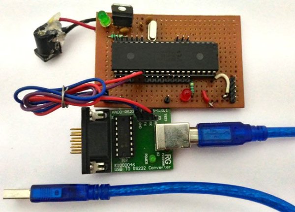
Openbench Logic Sniffer is an open source logic analyzer. It’s designed to support the SUMP logic analyzer software at the lowest possible cost. Download the source and design files from the Gadget Factory project page.

This project started in the comments on a post. Initial circuit design, PCB layout, development, and testing continued in the forum under the code name Project SUMP PUMP. Many, many people contributed ideas and advice, the Gadget Factory and Dangerous Prototypes coordinated circuit development and routed the PCB. We borrowed heavily from the Gadget Factory’s Butterfly Platform.

The Open Logic Sniffer is a purpose-built logic analyzer board designed to be low cost but high speed. It sacrifices a lot of the features you’d look for in a full-scale development board to achieve our primary goals:

  • 70MHz+ sample speeds
  • 32 channels
  • 16 buffered, 5volt tolerant channels
  • USB interface, USB powered
  • USB upgradable everything
  • Make it as DIY as possible
  • Make it as open source as possible
  • $30-$40 price range

We didn’t quite hit our initial price range, but we got really close.

You can get your own assembled Open Logic Sniffer at Seeed Studio for $45, including worldwide shipping. Continue reading about the design and collaboration below.
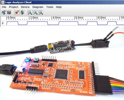
Prototype Openbench Logic Sniffer logic analyzerConcept Overview

SUMP is an open source Java logic analyzer client by Michael Poppitz. It consists of two parts, a VHDL logic capture engine for FPGAs, and a Java logic analyzer client. The latest development version of the SUMP client is available from SourceForge.net.

SUMP is a sampling logic analyzer. It reads the state of the input pins and stores the samples in internal ram. It then dumps the samples back to the computer client for analysis. The number of samples possible is limited by the RAM in the FPGA.

We like SUMP because it’s the best developed open source logic analyzer toolchain currently available. It has lots of professional features like multi-stage triggers, configurable pre-roll, external trigger and clock sync, and a few protocol analyzers (I2C, UART). It’s open source, so the potential to add cool new features is limited only by your imagination and coding skills.

SUMP is typically ported to a general-purpose FPGA development board. We took a different approach and designed hardware specifically for SUMP, while constraining costs wherever possible.

Other logic analyzers

Professional logic analyzers have tons of channels and super high speeds. We’re not trying to make a low cost DIY version of these tools, the OLS isn’t an alternative to these types of tools if you need to sniff 100MHz+ signals and have huge sample sizes.

Being an engineer’s tool, there are plenty of DIY logic analyzer designs. Parallel port based logic analyzers used to be all the rage, but with parallel ports and direct interrupt access disappearing from systems, these are just historical curiosities.

Another type of DIY logic analyzer is a microcontroller-based device. There are several with custom interfaces like the PIC Logix, Scanalogic, and AVR Logic Analyzer. The Bus Pirate works with SUMP. Microcontroller analyzers all have one thing in common: they’re really slow, usually sub-megahertz.

USB IO chip-based hobby logic analyzers are currently popular. We’ve always been fans of the Saleae Logic, the USBee is similar. These devices are just a USB IO chip like a CY7C68013A-56PVXC, with all trigger and processing logic done in software on a computer. The hardware part is just a datalogger. The top sampling speed is usually around 24Msps (24MHz), if the conditions on your USB bus are just right. They can take ‘unlimited’ samples because everything is stored on the computer. Current models tend to be 8 channels, more channels would reduce the maximum speed proportionately. These are commercial products with highly polished user interfaces, we don’t know of any that are open source.

The Open Logic Sniffer sits somewhere between hobby analyzers and professional analyzers. The OLS samples up to 200Msps, regardless of the USB bus traffic, and has true hardware triggers. The OLS has twice as many buffered channels as most hobby USB analyzers, and four times more channels overall. The major difference is that the OLS has a limited number of samples, while the hobby USB analyzers can theoretically take infinite samples. Most of our debugging is done with the first few hundred samples, so this feature isn’t usually important to our work, your situation may be different. Future versions of the OLS will definitely have more sample storage, and we can work an infinite sampling mode into a future firmware update too.

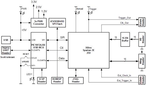
Click for a full size circuit diagram [PNG]. This circuit diagram, maintained by Uwe Bannow, shows the basic elements of the Open Logic Sniffer hardware. The FPGA captures logic samples from 32 input pins into internal RAM. The samples are dumped out a serial port for analysis on a computer. The open source SUMP logic analyzer client is used to capture and visualize the samples.

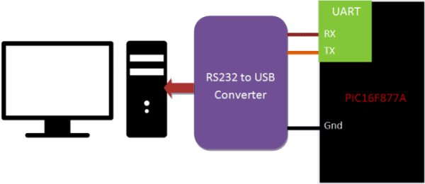
The FPGA only communicates over a serial port, so we used a USB microcontroller to convert the serial IO to a USB virtual serial port. The entire chain is upgradable through the USB connection. The microcontroller can program updated logic analyzer designs into the SPI flash data chip, and the microcontroller can also be updated from its USB bootloader.

We chose a USB microcontroller over a dedicated USB interface chip. A low pincount PIC was cheaper than most other USB bridge options. It’s USB 2.0 compliant, and can transfer data at up to 12Mbps. We’re using it with the completely open virtual serial port CDC interface, so it will work on almost any platform without proprietary drivers. The PIC can also implement other USB transfer protocols with a firmware update, faster connection methods can be supported when someone adds support for them to the SUMP client software.

Currently the SUMP FPGA design only transfers data over a 115200bps serial UART, the speed between the USB PIC and the computer isn’t a bottleneck. We routed several extra connections between the PIC and FPGA to implement a high-speed SPI interface in the future. The speed increase of an SPI interface can be supported in the SUMP client just by adding higher serial port speed settings.

An FTDI2232 chip was strongly considered as an alternative to the PIC. Here’s how we looked at it:

Benefits of the FTDI2232 with MSSP:

  • JTAG interface to debug the FPGA
  • SPI interface to program the ROM
  • SPI and UART interface to the FPGA

Cons:

  • Difficult to route
  • Expensive to place
  • Huge software development burden
  • Needs special drivers
  • USB interface not already supported by SUMP

With so much to accomplish already, major modifications to the client to work with untested hardware and custom drivers didn’t seem appealing. Not if the project were ever going to get finished. The PIC seemed like the best route for the first version.

Click for a large image of the schematic [PNG]. The schematic is divided into a microcontroller part [PNG] and a FPGA part [PNG]. These sections are where Ian and Jack initially split the design work. We used the freeware version of Cadsoft Eagle to make the circuit and PCB. Download the latest files from the Gadget Factory project page.

A Xilinx Spartan 3E field programmable gate array (FPGA) is the central component of the logic analyzer. The FPGA samples data from 16 buffered and 16 unbuffered IO pins, and stores the samples in internal RAM. The samples are later dumped out a serial UART to the PIC, and from the PIC to a computer via USB.

The basic FPGA schematic and PCB layout is taken directly from the Gadget Factory’s Butterfly Platform main board. The OLS shows how versatile the Butterfly Platform is as a development tool. The initial designs where first tested on the Butterfly Platform, and then we used the base design to create a unique, purpose-build hardware based on the prototype. You can get a Butterfly platform to build your own prototypes at the Gadget Factory for $99.

The FPGA (IC3) requires three different power supplies. The core requires 1.2volts and 2.5volts, and the IO pins run at 3.3volts. Each supply pin gets a 0.1uF decoupling capacitor (C11-26). We brought the JTAG programming and debugging connection to a header in the interior of the PCB. The JTAG header provides 2.5V to external JTAG programmers to satisfy the Spartan 3E’s requirements for 2.5V on the dedicated JTAG pins.

Several control and indication signals require special attention. INIT_B enables the FPGA when high, it’s held to 3.3volts with a 4.7K pull-up resistor (R6). The DONE signal goes high to indicate that the FPGA is configured and ready to use after a reset. It’s held to 2.5volts by a 300 ohm resistor (R1).

PROG_B, held at 2.5volts by a 4.7K pull-up resistor (R5), can be pulled low to put the FPGA in programming mode. The HSWAP pin (not shown) determines if all pins have pull-up resistors in programming mode. We grounded HSWAP so that all pins have weak pull-ups when PROG_B is low.

FPGAs are volatile programmable chips, they lose their configuration without power. The FPGA configuration, called a bitstream, has to be loaded into the chip each time it starts. We configured the FPGA to automatically load a bitstream from an SPI ROM chip by wiring the mode select pins as follows: M0(3.3volts), M1(0volts), M2(3.3volts).

The FPGA runs from a 50Mhz oscillator(Q2). This is a complete clock generation module, no external capacitors are required. The 50Mhz clock is doubled to 100Mhz by an internal Digital Clock Manager (DCM) to provide the 100Mhz clock required by the VHDL core.

Two LEDs indicate the FPGA status. The ARM LED indicates when a trigger is set and the device is actively waiting for the trigger. The TRIG LED indicates when a trigger has been activated. We used 390R current limiting resistors (R8, R9) on the prototype, but the assembled board should ship with 1K1 resistors to make the LEDs dimmer.

The FPGA IO pins are powered by 3.3volts, and can tolerate no more than a 3.3volt signal. The M74LCX16245DTR2G buffer (IC4) allows 16 buffered pins to sniff 5volt logic and can tolerate voltages from -0.5 to +7V. This chip is also powered by the 3.3volt supply, and it gets a 0.1uF decoupling capacitor (C9) on the supply pin.

The logic analyzer can sync with other test equipment and should allow OLS’s to be daisy chained together for more channels. It can be driven by an external clock and trigger, and it also outputs its internal clock and trigger. You can tap these signals from the some-what awkwardly placed pin block in the middle of the PCB. The external clock input had to be on an FPGA global clock pin, this was the best possible location to access it because no sensitive high-speed signals were routed across other traces.

Awing is an accessory for the Gadget Factory Butterfly Platform development board. It uses a standardized header and pinout. The header has 16bits of 3.3volt IO, and 2.5, 3.3, and 5volt power supplies.

We added a wing header to the OLS so it can use accessories developed on the Butterfly Platform, like a digital sampling oscilloscope. This has the added benefit of making the OLS compatible with a bunch of existing Butterfly Platform accessories.

The FPGA programs itself with a bitstream stored in a 4Mbit AT45DB041D SPI flash storage chip (IC2), we refer to it as a ROM. We previously demonstrated this chip with the Bus Pirate. It’s powered by the 3.3volt supply, and requires a 0.1uF capacitor (C10) on the supply pin. The XC3S250E bitstream will fit into a 2Mbit flash chip, but only 4Mbit chips were available when we sourced parts.

The ROM chip has an SPI interface that connects to the FPGA, the PIC microcontroller, and an external programming header.

  • The FPGA mode select pin configuration causes the FPGA to load a bitstream from the ROM chip. When the bitstream is finished loading, the DONE signal goes high, and the FPGA is programmed and active.
  • The PIC can (re)program the ROM with updated bitstreams. The PIC holds the FPGA PROG_B line low in this mode so the FPGA releases control of the ROM chip.
  • The external header can be used to program the ROM from a programmer. Place a jumper between the PGM and EN pins to manually place the FPGA in programming mode.

A PIC 18F24J50 microcontroller (IC1) is the interface glue. It has these functions:

  1. Provides a USB->serial connection from the SUMP Java client to the SUMP hardware in the FPGA
  2. Puts the FPGA in programming mode and updates the ROM with a new bitstream
  3. A USB bootloader can be used to update the PIC firmware

The 18xxJxx chips are really interesting, and seem like a hybrid of the 24F and 18F families. This PIC has the instruction set and 8bit core of the 18F family, but many enhanced features of the 16bit PICs. Half of the UARTs and SPI modules are assigned with peripheral pin select, it has flash configuration words, and it runs on 3.3volts, like a 16bit PIC.

The PPS features are really handy and make the clean layout of the PCB possible. The ROM SPI connection and FPGA UART connection are both assigned to custom pins with PPS. PPS can be used to implement a high-speed (10Mbit+) SPI connection between the PIC and FPGA in a future firmware upgrade.

The PIC is powered by 3.3volts, the supply pin gets a 0.1uF capacitor (C7). The USB peripheral has a separate 3.3volt supply pin that also needs a 0.1uF decoupling capacitor (C8). A 10uF capacitor (C4) is required for the internal 2.5volt core supply regulator.

An external oscillator provides an accurate USB clock, we used a 20MHz crystal (Q1) and two 27pF capacitors (C5, C6).

A 10K resistor (R3) holds the PIC reset pin high for normal operation, the RESET button (S1) grounds it to cause a hard reset. A second button (S2, R4) is available for simple user input.

The LED ACT is a general purpose indicator LED controlled by the PIC through current limiting resistor R7. The PWR (power) LED is connected to the USB supply though current limiting resistor R2, it illuminates whenever the board is powered.

We also brought the one of the hardware UARTs to a header. The pins are 5volt tolerant, and can be interfaced at up to 5volts without damaging the PIC. This header can be used for a ‘classic’ serial port connection. The board can also be powered through the UART header supply pins.

The board is intended to be powered by the 5volt supply from a USB port. Three regulators provide the three supply rails required by the circuit. All the chips require a 3.3volt supply (VR1), the FPGA also requires a 1.2volt (VR3) and 2.5volt (VR2) supply. As recommended by the datasheet, there’s a 10uF capacitor (C27) on the supply line, and each regulator has a 1.0uF capacitor (C1-3) on the output pin.

Numbering

The OLS has two different numbering schemes, one on the inside of the board and one on the outside of the board. The inside numbering scheme starts with zero on the buffered header. The outside numbering scheme starts with zero on the Wing header. Currently the numbering scheme can be selected by loading a bitstream that implements either numbering scheme. Future updates will support selecting the numbering scheme through the Java Logic Analyzer client.

We used the freeware version of Cadsoft Eagle to make the schematic and PCB. Download the latest files at the Gadget Factory project page.

The PCB is nearly the maximum allowable size in Eagle. All the components are surface mount, but we stuck with traditional through-hole headers. It took us an hour or two to solder each prototype board by hand.

We had boards made with the $50 Seeed Studio Fusion board service. This design probably would have been ready a bit sooner, but the PCBs were delayed about a month by the major Hong Kong Post Christmas mail rush.

Click for a full size placement image [PNG]. Uwe Bannow generously provided parts for the OLS prototypes. An extra special thanks to Uwe, his help was key to making this project what you see today.

Part
Quantity
Value
Package
C1-C3
3
0805
C4,C27
2
SMC_A
C5,C6
2
0805
C7-C26
20
0603
IC1
1
SO-28W
IC2
1
SO-08W
IC3
1
VQ100
IC4
1
TSSOP48
J1
1
SMD
LEDs
4
0805
Q1
1
HC49UP
Q2
1
OSC1
R1
1
0805
R2
1
0805
R3,R4
2
0805
R5,R6
2
0805
R7-R9
3
0805
S1,S2
2
DTSM-6
VR1
1
SOT23-5
VR2
1
SOT23-5
VR3
1
MIC5205-1v2 (MCP1801T-1202)
SOT23-5
JP7,JP8
2
1X09

Prototype Openbench Logic Sniffer logic analyzerSUMP FPGA design

Get the latest project files from the Gadget Factory project page. The original SUMP project is licensed under the GPL, you can get it at SUMP.org.

OLS Design Changes

The OLS uses the open source (GPL) SUMP logic analyzer VHDL design. It’s synthesized with the free Xilinx ISE Web Pack tool suite. Our design is based on Jonas Diemer’s Spartan 3E SUMP port [ZIP]. The following modifications were made for the OLS hardware:

  • A new ucf (User Constraint File) was generated to map the pins of the FPGA to the layout of the OLS board and to support multiple numbering schemes.
  • Support for outputting the sample clock to an external pin was added.
  • Support for adding an external pin as a trigger was added.
  • Added support for Trigger and ARM LED’s.
  • Files for multiple BRAM memory configurations were added. The files were generated with the Xilinx Core generator and are Xilinx specific.

Memory

The OLS utilizes BRAM (Block Ram) that is embedded inside the Spartan 3E FPGA, the included XC3S250E chip has 216K of BRAM available. There are six bitstreams that allocate the available memory into different combinations of memory depth and sampling channels. Currently the following memory/channel configurations are available:

  • 32 channels with 4k sample depth.
  • 16 channels with 8k sample depth.
  • 8 channels with 16k sample depth.

You may have noticed that the above numbers don’t add up to the 216K of BRAM that is available. With 8 channels we should be able to get 216k/8 = 27k samples. The first issue is that the published size of 216K of BRAM includes parity bits, without parity bits we actually have 192K of BRAM available. The second issue is that the Sump design is setup to require a power of 8 for its sample depth, so until the Sump design can be modified we are stuck with the above power of 8 sample depths. Once these two issues are resolved the possible memory/channel configurations will be:

  • 32 channels with 6k sample depth.
  • 16 channels with 13k sample depth.
  • 8 channels with 27k sample depth.

Our future design plans do include working on adding 32-64Mb of SDRAM memory.

Bitstreams

The output of the Xilinx Webpack synthesis tools is a bitstream file that is used to configure the FPGA. We convert the bitstream (*.bit) file to an Intel Hex format (*.mcs) using the Xilinx Impact application. The bitstream is then loaded, by the PIC, into the Atmel SPI Flash chip. When power is applied to the OLS the FPGA configures itself by loading the bitstream from the SPI Flash chip.

There are currently six different bitstreams that provide for 3 different memory configurations and 2 different numbering schemes. Currently, the bitstreams have to be loaded with the pump-loader executable. Future revisions will load the desired bitstream from the Java Logic Analyzer client.


For more detail: Prototype Openbench Logic Sniffer logic analyzer

The post Prototype: Openbench Logic Sniffer logic analyzer using pic microcontoller appeared first on PIC Microcontroller.

Stepping Into the 16-bit World with the Microchip 16-bit PIC24F16KA102 Family Microcontroller

$
0
0

One of the commonly asked questions when we move to the bigger and powerful 16-bit microcontroller is do we really need it? As the 8-bit microcontroller is already suite almost all of our needs from a simple blinking LED to more sophisticated embedded application such as robotics. Despite the debate whether to use the 8-Bit or 16-Bit microcontroller or perhaps just go straight to 32-bit microcontroller in our embedded system design, first I will show you the Microchip PIC18F25J11 (8-Bit) and PIC24F16KA102 (16-bit) basic comparison.Stepping Into the 16-bit World with the Microchip 16-bit PIC24F16KA102 Family Microcontroller

I use the Microchip PIC18F25J11 for the comparison as this microcontroller is considered as the 8-Bit highest end class microcontroller equipped with Microchip nanoWatt XLP technology while the Microchip PIC24F16KA102 is considered as the 16-bit entry level class microcontroller also equipped with Microchip nanoWatt XLP technology. Both microcontrollers have a build in hardware RTCC (Real Time Clock and Calendar), I2C, SPI and CTMU (Charge Time Measurement Unit) for capacitance sensing.

Now here my opinion from the electronics hobbyist perspective, things that we always consider when learning a new microcontroller are how easy to quick prototyping it on the breadboard, how much the cost and the last is the development tools to be used. From the basic comparison above you’ve noticed that for the learning purpose these two types of microcontroller are almost identical. On the other hand let’s consider the advantages of learning the 16-bit microcontroller; the PIC24F16KA102 microcontroller families share the same architecture as the well known Microchip dsPIC (digital signal controlling) microcontroller families, therefore by learning the 16-bit PIC24F16KA102 microcontroller family will open your knowledge and richer your experiences to more advance application of the embedded world system and surely you will love and enjoy it.

…to explore a new 16-bit microcontroller world… new datasheet… and …new programming… to boldly go when the only true electronics hobbyists dare to go…

On this tutorial we are going to step into the 16-bit embedded world and I will use the Microchip PIC24F16KA102 microcontroller as our learning tools. Actually Microchip has a nice product to help you quickly learn the PIC24F16KA102 families featuresSchematic Stepping Into the 16-bit World with the Microchip 16-bit PIC24F16KA102 Family Microcontroller

Ok now let list down the necessary electronics components and supported software for our stepping into 16-bit world tutorial and make sure you have the Microchip PIC24F16KA102 microcontroller datasheet near you:

1. Resistors: 330 Ohm (9), 470 Ohm (1) and 10K (2)
2. Capacitors: 0.01uF (2) and 0.1uF (2)
3. LEDS: 3 mm Blue LED (8) and 3 mm Red LED (1)
4. One Microchip 16-bit PIC24F16KA102 microcontroller
5. Two momentary push button
6. One Breadboard and some breadboard’s jumper cables
7. One 2xAA Battery Holder with the 2x AA Alkaline battery (3 volt) for powering the circuit
8. Microchip PICKit3 programmer (used in this project)
9. Microchip MPLAB IDE version 8.47 and Microchip C30 Compiler version 3.30
10. Microchip PIC24 Reference Document: PIC24F16KA102/101 datasheet, AN39703a (CPU), AN39711b (I/O), AN39704a (Timer), AN39705b (ADC)

For more detail: Stepping Into the 16-bit World with the Microchip 16-bit PIC24F16KA102 Family Microcontroller

The post Stepping Into the 16-bit World with the Microchip 16-bit PIC24F16KA102 Family Microcontroller appeared first on PIC Microcontroller.

Introduction to the Embedded System with PICAXE Microcontroller

$
0
0

These days we are living and surrounding by many tiny computers called embedded products. Unlike the general purpose desktop computer that we use for browsing or typing our email, this tiny computer is designed to do only a limited specific task. We could easily found this embedded product just about anywhere such as home appliance (e.g. washing machine, refrigerator, microwave oven, TV/DVD), personal gadget (e.g. cell phone, MP3 players, digital camera), car (e.g. anti lock brake system, GPS navigation, alarm) and many more. The tremendous use of the embedded products in our daily life make the embedded system become one of the most important and interest subject to be learned.Introduction to the Embedded System with PICAXE Microcontroller

Now come to the most asked question “How do I start it?” Actually when we learn the embedded system; we learn two things at the same time, the first one is the hardware which usually a microcontroller and the second one is the software to program the microcontroller to perform the desire task. Therefore most of the microcontroller manufacture already provides this learning tool all in one package (starter kits) to introduce their product to the microcontroller newcomer. Unfortunately most of this learning tool is aimed for the people that already have an adequate knowledge both in hardware and programming language.

Considering this need, many companies and the open source community start to offer their own embedded system development framework version, where this framework mostly aim for student, hobbyist and even to the professional.

Among these embedded system learning and development framework I found that the PICAXE from Revolution Education Ltd in UK (http://www.rev-ed.co.uk/picaxe) is one of the best in terms of price and ease to be used. Equipped with the free sophisticated PICAXE Programming Editor to program, debug, simulate and download the code to the PICAXE microcontroller; therefore this makes the PICAXE framework is a perfect choice for the embedded system newcomer.

The PICAXE Microcontroller

Unlike the other BASIC interpreter framework mention above which use the EEPROM to store the program, the PICAXE is a stand alone microcontroller solution, where both of program and the BASIC interpreter firmware is stored in the PIC microcontroller own memory (FLASH and/or EEPROM). Therefore the PICAXE only required a very view external electronic component in order to make it work.Schematic Introduction to the Embedded System with PICAXE Microcontroller

In fact you could drop the 180 ohm resistor (connect pin 19 directly to TX) shown on the above schematic, which left only two resistors (22K and 10K) to make this PICAXE microcontroller a fully function embedded learning system. Connecting the RS232 DB-9 female connector to your computer COM port or USB to RS232 converter and you are ready to program this PICAXE microcontroller.

For more detail: Introduction to the Embedded System with PICAXE Microcontroller

The post Introduction to the Embedded System with PICAXE Microcontroller appeared first on PIC Microcontroller.


TRACK CONTROLLER FOR AWANA® GRAND PRIX using PIC16F628

$
0
0

Introduction

This project is for the hobbiest who wants to build a measurement and display unit for an Awana Grand Prix® track (also known as a Pinewood Derby track.)

TRACK CONTROLLER

The racetrack for which I designed this unit is a 4-car track. A car is approximately seven inches long, is released by a gate at the starting line, rolls down the ramp by gravity, and crosses the finish line in approximately five seconds. This was designed for Christ Memorial Church, Williston, Vermont, USA.

This circuit is contained in three places: in the controller/display box, in the finish line “bridge” unit, and at the start gate. The power supply, the controller/display box, and the start gate switch/servo each connect to the track finish line “bridge.”

The controller box also has a 9-pin serial jack for connection to a computer with appropriate software. For computers lacking a serial jack, RS232-to-USB adapters may provide connectivity. Recommended and tested race management software is “GrandPrix Race Manager” from GrandPrix Software Central. This software is well-written by Randy Lisano, highly configurable (easily customized to work with this track controller) and produces a full-screen image that is very suitable for use with a video projector.

C code
Schematic
My other projects
Questions? Please email me.     Jon Fick

TRACK CONTROLLER Schematic

Features

Timing is initiated either by pressing the push button or by computer control. The controller waits for one or more cars to cross the finish line and displays the order of finish as well as elapsed timing information.

 Code:

// RACE START CHECKS.  These are defined at compile time.
// 0 = no checks,    1 = finish line check only,    2 = start gate and finish line check
#define START_CHECKS     1

/***************************************************************************
AGPV030709.C

This program controls an Awana Grad Prix racetrack.
Times out at 9.999 seconds.
Uses a start switch (local N.O. pushbutton)
and a remote gate switch (N.C.)
and a remote gate actuator.
This version can mask lanes.
With serial communication.
With First Place LED atop each lane.

Elapsed time is 1mS interrupt driven.
Serial communication is interrupt driven, 9600-8-E-1.

WORKING CODE, RACE VERSION!!!

                         +5                             +5
                          |                              |
                         14                              2
                      ----------                     ----------
 -Start---ProgM----4-|          |-10-------------11-|DB4 Vdd   |
 -StopR-----------17-|          |-11-------------12-|DB5       |
 -StopB-----------18-|          |-12----ProgC----13-|DB6       |
 -StopG------------1-|  16F648  |-13----ProgD----14-|DB7     Vo| 3----20K pot
 -StopY------------2-|          |-9---------------6-|EN  LCD   |
 -RemSw------------3-|          |-6---------------4-|RS        |
        6MHz XTAL-16-|          |-7--Rx             |          |
              TAL-15-|          |-8--Tx             | RW   Vss |
                      ----------                     ----------
                           5                           1   5
                           |------------ProgG          |   |
                          Gnd                         Gnd Gnd

**************************************************************************/


For more detail: TRACK CONTROLLER FOR AWANA® GRAND PRIX using PIC16F628

The post TRACK CONTROLLER FOR AWANA® GRAND PRIX using PIC16F628 appeared first on PIC Microcontroller.

Using PicBasic with the PIC16F84 PIC Microcontroller

$
0
0

This article shows how to use the PIC16F84 microcontroller with PicBasic to design a quick & effective, serially controlled, I/O-Expander.  Using PicBasic makes developing handy single-chip devices like this extremely simple.

If you’re spending all your time programming in assembler, you’ll appreciate how simple PicBasic is to use, and how easily you can create single-chip solutions like this one in mere minutes.

This project uses only a few of the instructions that come with PicBasic, but serves to show how easy PicBasic really is.  It also shows how PicBasic strongly resembles programming the BASIC Stamp.  Here we are using the serin command, and a couple if then statements to design a simple serially controlled I/O-expander that can be used to increase the I/O capabilities of other PIC microcontrollers or the BASIC Stamp.

Using PicBasic with the PIC16F84 PIC MicrocontrollerOne feature that PicBasic offers with the serin command is the ability to use a qualifier.  Using this technique, we can force our serial I/O-expander to wait for a specific qualifier before accepting other data from the serial-pin.  This helps to ensure that our I/O-expander isn’t false triggered by line noise, or other interference.  It also helps us to synchronize the incoming data and make sure we receive everything in the correct order.

The code for this project waits for the qualifying number 254 to arrive on the serial-pin.  Once the qualifier is received, the program will then accept the remaining data, and use this information to control the output-pins.

The code for this project was kept as simple as possible to help beginners understand how it works.  If you’re already an experienced programmer, you may find the simplicity of the idea to be a starting point for much larger, and more sophisticated designs with a similar purpose for your own applications down the road.

Note:  This project can be used with the PC serial port, the BASIC Stamp, and other PIC microcontrollers.  The ability to (directly) interface the PIC microcontroller to the PC serial port eliminates the need for expensive RS-232 conversion ICs such as the MAX-232.  A single 22K resistor is all that’s required to complete the PC interface.

To control our serial I/O-expander, we only need to send it a three-byte string of serial data.

bullet

The qualifier number 254.

bullet

The relay number we want to address & control.

bullet

The logic state we want the relay output-pin to go to.

You can use this project as a simple I/O-expander, or to control up to 12 individual relays directly interfaced to your PC, a BASIC Stamp, or just about any type of microcontroller capable of sending asynchronous serial data.  It has quite a few uses for many various applications, and it’s so incredibly simple to build, it can easily replace much more expensive solutions.

The BASIC Stamp II Code

'' ====== Program to exercise the PIC16F84 serial relay module ======
' This program sends serial data out pin 0 of the BASIC Stamp II
' or the Wedge prototyping board to exercise the PIC16F84 I/O
' expander/relay control module.  Data is sent 2400,N,8,1 through
' a 22K resistor in series with pin RA.4 [the serial input pin]
' of the I/O expander/relay control module.

time 	var byte ' Change byte to "word" for longer delay times.
synch 	con 254
relay 	var byte
stat 	var byte
loops 	var byte
time = 250
start:	for relay = 1 to 12
	    stat = 1
	    serout 0,16780,[synch,relay,stat] 
	    pause time
	    stat = 0
	    serout 0,16780,[synch,relay,stat]
	    time = time - 1
	    if time = 0 then reload
	next
	goto start

reload:
	time = 250
	goto start

Using PicBasic with the PIC16F84 PIC Microcontroller SchematicThe individual outputs are simply addressed as 1 through 12.  The logic states are a 1 or 0 depending on the logic state you want the output-pin to go to.  The BASIC Stamp II sample code above will exercise the I/O-expander very quickly by sending a series of commands to the I/O-expander causing the output-pins to toggle from 1 to 0 extremely fast.

The pause is only 250mS to start with.  The line time = time – 1 quickly decrements the remaining pause time down to 0.  This is a fun program to run with this project, and it shows how fast the PIC can operate without missing incoming serial data.  The program will cycle through all 12 I/O-pins, and return to the beginning once finished.  To test your circuit, hookup 12 LEDs to the output-pins of your I/O-expander through 470 ohm series resistors and watch it blaze through the count.


For more detail: Using PicBasic with the PIC16F84 PIC Microcontroller


The post Using PicBasic with the PIC16F84 PIC Microcontroller appeared first on PIC Microcontroller.

Cheap PIC controlled Helmet Camera using Sony LANC (Good for Extreme Sports) using PIC16F690

$
0
0

Cheap PIC controlled Helmet Camera using Sony LANC (Good for Extreme Sports)

This Instructable will show you how to make a cheap Helmet Camera which can be controlled via a remote so your main camera can stay safely in your ruck sack.

The controller can be attatched to one of the shoulder straps of you ruck sack, and will allow you to Record and Stop the camera as well as being able to switch the ‘bullet’ camera on and off also.

This is perfect for people who want to film extreme sports such as bmxing, snowboarding, skateboarding etc. from a first person perspective.

The picture below shows the bullet camera and remote controller along with the main camera adn battery pack.

Helmet Camera

How it works.

It is fairly simple to connect a small ‘bullet’ style camera to your camcorder and get the camcorder to film what the mini camera is ‘seeing’, but I wanted to be able to control the record and stop fuctions of the camcorder without taking out of my bag everytime.

After a little investigation, I found that Sony camera have a LANC connection on them which can be used to control the camera and also give information about the what the camera is doing. This is great, becasue when you remotely press the Record button, you can read the data from the LANC cable to find out if the camera is actually started recording, and have a record LED illuminate on your controller.

The mini camera cost only 15 pounds from ebay
The 2.5mm stero jack was about 1 pound
and the other bits and pieces were less than 5 pounds

So for about 20 pounds, you can have a a fully working, remote control helmet cam.

My controller is very simple. It has a Record button, a Stop button, a power switch for the mini cam and 3 LEDs. (Minicam power, Main camera power and a record indicator). This is all I needed for my project, but the source code I have supplied is pretty straight forward and can be adapted to allow you to control anything on the camera.


I have added another step, Step 4, it is an update that gives an indication of low battery and end of tape)

Pictures:

Picture 1 – The prototype (with 8 LEDs to help debug my program)
Picture 2 – A close up of the ‘bullet’ camera and controller

The circuit diagram

The circuit is very basic.

Schematic of Helmet Camera
– The PIC is powered directly from the LANC cable.

– The Minicam is powered from a 12 volt battery pack via a switch

– There are 2 push buttons for Record and Stop

– 3 LEDs are used to show you the status of the camera

PIC connections:

RA0 – LANC from the camera
RB7 – Record LED
RB4 – Record button
RB5 – Stop button

(Please note, Step 4 is an update to this circuit, the power LED is connected to RA5 and there is a different source code)


For more detail: Cheap PIC controlled Helmet Camera using Sony LANC (Good for Extreme Sports) using PIC16F690

The post Cheap PIC controlled Helmet Camera using Sony LANC (Good for Extreme Sports) using PIC16F690 appeared first on PIC Microcontroller.

The ‘One Chip Spinning RGB POV Display’ with conversion software using PIC18f4680

$
0
0

The ‘One Chip Spinning RGB POV Display’ with conversion software.

If you have been on the look out for a project that combines, RGB LED’s, a motor, a microcontroller and a ridiculous amount of hot melt glue, then you have certainly come to the right place.

One Chip Spinning RGB POV Display
Allow me to introduce the ‘One Chip’ Spinning RGB POV Display

This project allows you to create (with minimal components) a fantastic customizable display capable of displaying graphics, animations and text. You can scroll your graphics from top to bottom or use it as a scrolling message display, scrolling from right to left.

The project uses just one chip, eight RGB LED’s and a handful of other components to paint animations in ‘mid-air!’ Plus, together with the included graphic conversion software (download link in step 2) you can easily create your own animations because the software creates all the code for you.

So please, read on and enjoy!

Step 1

Get your required parts and tools.

Before we set out on this venture, you will need both the components and tools.

Parts List:

1x PIC 18f4680 microcontroller
1 x 40 pin IC socket (optional – to house the microcontroller)
8 x Common cathode RGB LED’s
24 x 100 ohm resistors (any wattage)
1 x 0.1 uF capacitor (optional)
2 x 100 uF capacitors
1 x 7805 (5 Volt Regulator)
2 x 10k ohm resistors
1 x hall effect sensor / hall effect switch
1 x 5 pin header (to plug in the pickit2 programmer)
1 x small rare earth magnet (to be used with the sensor)
1 x screw in type mains wiring terminator (See last photo – you get these from a hardware store)
1 x 12v motor
1 x motor (any motor that you can destroy for parts – I.E. the graphite brushes)
1 x 12v powersupply (for the motor)
1 x 7.5 volt power supply (for the POV display – can be upto about 18v)
1 x (5.5cm x 5.5cm blank pcb – aka blank copper clad) – this will be used to transfer power to the display
Holt Melt Glue Sticks
Solder
Veroboard / experimenters board
Thin enamel wire (see pic)
Standard single core wire (Like they use in network cable)

Tools:

– Soldering Iron
– Screw Driver
– hot melt glue gun
– Stanley knife
– side cutters
– pliers
– pickit2 programmer
– desoldering tool (solder sucker or solder braid – just in case!)
– computer running windows
– swordfish basic compiler (this is a free download – it compiles the code for the microcontroller)
– POV Image Converter (Software that I have made, download link is included in the instructable)Now that you have all of that, let’s get into the construction.

Step 2

Downloads

First and foremost, you will want to download the schematic so that you are not building this blindly, and perhaps you may want to experiment with the conversion software also. All these downloads are provided here:

Please read the readme.txt file for instructions on how to install the software.

Click this link to download the schematic:
http://www.bradsprojects.com/forum/download/file.php?id=297

Click this link to download the scroll down conversion software:
http://www.bradsprojects.com/forum/download/file.php?id=294

Click this link to download the scroll left conversion software:
http://www.bradsprojects.com/forum/download/file.php?id=290

Click this link to download swordfish basic (free version):
http://www.sfcompiler.co.uk/downloads/SwordfishSE.exe

Step 3

Let construction commence!

Now the beauty about this project is that you don’t have to make it exactly how I have made it.

my original intention was just for me to see how small a board I could fit this project onto. But as you will see, there is plenty of space to work with when we attach the main arm that connects the display to the motor. So by all means, have a look at my design – but there are certainly other ways (simpler ways) of achieving the desired outcome.

I have cut my board so that I have 26 holes by 10 holes.

Step 4

Solder in the LED’s and cut some tracks

I have used surface mount LED’s just to see how they would go (I have previously used through hole LED’s in a past project)

Solder the Red, Green and Blue connections to the board.

The three connections on the top are the cathodes. (this may differ for your LED’s – give them a quick check with your multimeter to verify)

You will also notice I have cut a line through the tracks connected to the LED’s. This is so we can solder in some series resistors to limit each LED’s current.

IMPORTANT NOTE: You need to make sure that the bottom LED is connected as your least significant LED. I.E. this led will connect to PORTA pin 0, PORTB pin 0 and PORT D pin 0. You then work your way up from there. Follow the schematic and you will be fine = )

Step 5

Solder in your resistors.

I have also used surface mount resistors to keep my project small, you may very well want to use through hole to make things a little easier.

The resistors solder in over the tracks that you have just cut.

Step 6

Cut some more tracks and solder in a ground wire.

Solder in your resistors
Now that the resistors are in place, you will want to cut another line of tracks on the other side of these resistors, getting them ready to solder to the microcontroller. – see the first photo

Once done, get a length of uninsulated wire and solder it along the length of the LED cathodes. then solder it to the veroboard (this will be our ground connection) – see second photo

Step 7

Time for a quick test.

Progressive tests are always a good thing, so let’s do one.

Grab a 5 volt power supply and solder your negative end to our ground connection. then with the positive side, connect it to each resistor one at a time – you should have each LED light up with the respective color as you work your way through all 24 connections.

It’s nice to pick up on faults before we get to carried away!

Step 8

Install the microcontroller, socket and cut some more tracks.

Now it is time to solder in the socket which will house the microcontroller. Or if you wish, just solder the microcontroller straight in (if it is to be a permanent arrangement).

Then you will need to cut a line of tracks so that we do not short each end of the microcontroller together. – see the last photo.

For more detail: The ‘One Chip Spinning RGB POV Display’ with conversion software using PIC18f4680

The post The ‘One Chip Spinning RGB POV Display’ with conversion software using PIC18f4680 appeared first on PIC Microcontroller.

Record Infrared Codes of Any Remote Control Unit for Usage with Linux Infrared Remote Control (LIRC) on Raspberry Pi

$
0
0

Introduction

The remote controls that are orphaned when the device they control stopped working are reusable on your Raspberry Pi. After completing this instructable, you may be interested in trying out the following instructables:

Reuse Unwanted Remote Control to Shutdown and Reboot Raspberry Pi

Reuse Unwanted Remote to Launch Graphical Application in Raspberry Pi

Scope

This instructable will show how to use program irrecord to:

  1. Capture infrared codes of any remote control
  2. Map the infrared codes with Linux Infrared Remote Control (LIRC) events

Target Readers

Anyone with Raspberry Pi that has infrared (IR) interface)

Any remote controlRecord Infrared Codes of Any Remote Control Unit for Usage with Linux Infrared Remote Control (LIRC) on Raspberry Pi

Step 1: Add Infrared Interface to Your Raspberry Pi

Complete the steps in my instructable of the above.

Step 2: Install Linux Infrared Remote Control (LIRC) package

The program irrecord is provided by the LIRC package.

Complete the steps in my instructable of the above.

Step 3: Test whether the remote control unit is transmitting any IR signal

Complete the steps in my instructable “Use Raspberry Pi To Test Your Remote Control”Record Infrared Codes of Any Remote Control Unit for Usage with Linux Infrared Remote Control (LIRC) on Raspberry Pi schmatic

Step 4: Record infrared (IR) codes of the remote control and map it to LIRC events

Get your remote control unit ready

Open terminal emulator of Raspberry Pi.

Stop the LIRC daemon

Run the program irrecord

When the irrecord program wizard ask you to map key names, open another terminal emulator and list all the possible key names available in LIRC so that you can choose the best one that fits your requirement. The output of the command below is shown in the screenshot

Finally, the irrecord program will process your input and create a configuration file ~/my_remote_control.conf as shown in the third screenshot.


For more detail: Record Infrared Codes of Any Remote Control Unit for Usage with Linux

Infrared Remote Control (LIRC) on Raspberry Pi

The post Record Infrared Codes of Any Remote Control Unit for Usage with Linux Infrared Remote Control (LIRC) on Raspberry Pi appeared first on PIC Microcontroller.

Viewing all 223 articles
Browse latest View live


<script src="https://jsc.adskeeper.com/r/s/rssing.com.1596347.js" async> </script>