Quantcast
Channel: Other Projects - PIC Microcontroller
Viewing all 223 articles
Browse latest View live

Dspic-Servo Project using PIC30F4012 microcontroller

$
0
0

Project Description

This project was developed as an inexpensive way to drive small dc brushed motors as positioning servos for use on a desktop sized CNC machine. The board is interfaced to the PC through 2 pins of a parallel port. The drive signal on these pins is known as quadrature drive.

Dspic-Servo

The power stage consists of a power op amp driven in constant current mode. The internal PIC processor ( a 30f4012 from Microchip ) is programmed in C through the C30 compiler and the Microchip IDE. The servo loop parameters are programmed through a serial port connection and are saved in the dspic eeprom. Once set for a particular drive, they should not need to be changed.
A YouTube video by Ted Maczulat.

The serial programming interface is used to tune the PID and other servo loop parameters to optimize the performance in a particular application. The serial port runs at a fixed baud rate of 9600N81. Any terminal program such as minicom, gtkterm, or hyperterminal may be used to talk to the dspic-servo. On powerup you will see the following:

Powerup...i/o...uart...timer...pwm...pid...encoder...capture...done

dspic-servo by L. Glaister
(c)25-Sept-2006 by VE7IT

using setup from eeprom.. ? for help

Current Settings:
servo enabled = 1
(p) = 0.020000
(i) = 0.000000
(d) = 0.000050
FF(0) = 0.000000
FF(1) = 0.000000
dead(b)and = 1.000000
(m)ax output = 2.500000
(f)ault error = 1024.000000
(x)pc cmd multiplier = 3
(t)icks per servo cycle= 10

To change a value, type the cmd letter/number and then a value for example:

p0.03

The current values will be redisplayed with the new value set. The p,i,d, ff0 and ff1 values are standard loop gain parameters. You can reference the source code for a better explanation. The deadband parameter is the number of encoder counts the servo can be out of position without the servo loop taking any corrective action. The max output is the maximum current output allowed in amps and should be set for the particular motor you are using. This number can be up to 7 amps. The fault error parameter is used to set the number of counts the servo can be out of position before the drive gives up and indicates a drive fault. This is used to detect crashes and jammed axis or input command conditions beyound the capabilities of the motor. The pc command multiplier is useful for cases where you have a high resolution encoder on the motor and a PC that is limited in the number of pulses/second it can output. For most operation this number will be set to 1, but if you have trouble reaching the top speed you need from the drive, it may be helpful to set this number to a higher value. The internal servo loop works by keeping 2 counters. The first is the commanded position from the PC, the second is the actual position from the encoder. The servo loop of the drive attempts to keep these 2 numbers as close as possible to each other.


For more detail: Dspic-Servo Project using PIC30F4012 microcontroller

The post Dspic-Servo Project using PIC30F4012 microcontroller appeared first on PIC Microcontroller.


Rotating Sprocket Wheel Generator using PIC16F84

$
0
0

Background

My friend Arthur, in his lifelong quest for circuits that don’t really do anything useful, but are really neat nonetheless, built a really neat Lissajous pattern generator. This Lissajous pattern is not your traditional circle, oval, or figure-8, it is a circle with varying amplitude, in a pattern that makes it look like a sprocket. Not satisfied with that, he also made it so that the sprocket rotates.

Wheel Generator

An interesting side-effect is that this circuit very clearly shows some of the shortcomings of digital oscilloscopes. Whenever an oscilloscope salesman comes around, he whips out this box with a switch and 2 BNC jacks. It has been known to render speechless the best salesmen from HP and Tektronix. They usually dismiss it as a toy, but I think that is just because they have to follow the party line: Analog scopes are dead. I have seen a digital scope or two accurately mimic the analog, most notably the Digital Phosphor scopes from Tektronix, but in general, the RSWG breaks digital scopes.

I moved to another job about 1500 miles away from where Art spends his time being surly, making cool circuits and serenading passersby with his Theremins. After a short time at my new lab I was called upon to specify some oscilloscopes. I decided that I needed my own RSWG. Arthur has been so kind as to publish theschematics and theory behind his RSWG. His circuit works great, but it is pretty complex, and the construction would tax my patience, since he has managed to construct his RSWG with nothing but discrete ICs and a handful of ancillary components.

I, on the other hand, like most engineers, decided I would rather start from the ground up and roll my own. My first objective is to reduce parts count. When I was working for the Army, I made a really neat circuit that was among other things, a frequency synthesizer. It would generate two sine-waves in quadrature with a minimum of external components (just a D/A converter). The problem with re-using that code was that I no longer had easy access to an Altera development system. On the other hand, I had been using a PICStart+ for some of my other projects at the lab, and if all else fails, I would have the POHPIC Programmer that I designed myself. I decided to try basing it on a MicrochipPIC, the 16F84. The ‘F84 has some features that are completely unnecessary for this project, notably non-volatile memory. But the big advantage of it is that 1) I had some handy, and 2) the flash program memory supports my style of simulate, burn, crash, repeat embedded programming, without the hassle of an EPROM eraser. This code would easily port over to one of the PICs without flash memory (such as the 16C61).


The Circle

First of all, I had to see if I could even draw a simple circle on the oscilloscope screen. To do this, you must put out 2 sine waves in quadrature (a fancy term for 90° out of phase). When you feed these two waves into the X and Y inputs of an oscilloscope, you draw a circle on the oscilloscope’s screen.

A sine wave is about as analog a signal as you can get. In case you didn’t realize it, the ‘F84 only has digital outputs, so I needed to convert a digital set of values to an analog voltage. I could use a D/A converter, but I didn’t have any handy. What I did have handy was a huge number of precision resistors. Just the recipie for an R/2R resistor ladder, which is what you see to the left. To use an R/2R D/A network, you place the digital word you want to convert to an analog voltage on the input pins. The closer the 1s are to your supply voltage, and the 0s are to ground, the better, since these voltages are added together through these resistor dividers to generate the analog voltage. The most significant bit goes on the upper-most input of the diagram to the left, and the least significant bit goes into the bottom-most input.

The 16F84 has 13 outputs. All 13 can serve as inputs, but only 12 are normal outputs, one is an open-drain. An open-drain output has no active pull up- you have to provide an external (passive) pull up. Since the ‘F84 is CMOS based, this leaves us 12 outputs that have good, low impedance 1’s or 0’s. We want two channels, 12/2 = 6 bits/channel. Using the rough approximation of 6 dB/bit, 6 bits/channel * 6 dB/bit gives us approximately 36 dB/channel of dynamic range. This is still very visible on a scope, so I needed some filtering.


For more detail: Rotating Sprocket Wheel Generator using PIC16F84

The post Rotating Sprocket Wheel Generator using PIC16F84 appeared first on PIC Microcontroller.

PBUS – an RS485-like multi-drop bus with half duplex serial protocol

$
0
0

overview

There are three PIC source versions:

  • PB12 is for 12-bit slave devices without interrupt
  • PBUS is for slave devices with an interrupt, software UART implementation
  • PB628 is for slave devices with an intterupt and a free hardware UART

PBUS assigns a unique device ID in the range 1-f for every controller on the bus. The maximum number of slave devices on one bus is maximized in 15. Current protocol is one master, multiple slaves.

The implementation uses 2400 baud half-duplex serial communication. Only 2 wires (GND and PBUS signal) are needed to interconnect devices using their own power supply. Using a higher speed or other protocols on the same PBUS is possible, since slaves won’t respond to packets they can’t interpret.

PBUS - an RS485-like multi-drop bus with half duplex serial protocolpacket structure

Packets consist of 8-bit bytes. All packets contain at least 3 bytes. Maximum length is 18 bytes.

byte offset bits name description
0 7-4 DEVID destination device PBUS ID
0 3-0 LEN optional data length (0 means packet is 3 bytes, no optional data)
1 7-0 CMD MASTER command or SLAVE response code
2 7-0 DATA[] optional data, length is given in LEN (LEN=0 means no data)
2+LEN 7-0 CHKSUM packet checksum. Added to the packet bytes sum will result a sum of zero

PBUS timings

Master devices generates a 8500 usec gap on the bus before transmitting a PBUS packet. This is for synchronization of all listening receivers. Receivers can expect to see a min. 4900 usec, max. 21200 usec gap. Packet bytes must be sent without interruption. Packet reception will be reset if a gap longer than 200 usec is detected. After the request packet is sent, the master waits up to 1000 usec for a reply from the addressed slave. Slaves check received packets in this order:

  • check for a valid checksum. If invalid, drop packet and go back listening
  • check for own device ID. Ignore all other IDs without response
  • if the command is not implemented, ignore the packet and go back listening
  • process the command and generate a response with a destination device ID 0

PBUS commands

PBUS handlers will implement some commands internally.

Commands implemented by ALL sources:

dev cmd
code
cmd
parameters
description
M 5e CVER (check node version)
S 60 ROK <pbus version> [main version] [optional string describing node] current nodes do not return the optional string by default
M 5f CPING [optional data] (test if a node is present and the link is up)
S 6f RECHO [optional data echoed] PB12 sources will not echo the supplied ping data back

PBUS - an RS485-like multi-drop bus with half duplex serial protocol SchematicCommands implemented by sources except PB12:

dev cmd
code
cmd
parameters
description
M 58 CNOOP (no operation)
S 60 ROK
M 5b CLAST (repeat last response)
S (copy of the last response packet sent)
M 5c CRES (reset statistics counters)
S 60 ROK
M 5d CSTAT (get PBUS statistics)
S 60 ROK <e1> <e2> <e3> [optional counters] The CRES and CSTAT commands can be disabled.

Meaning of counters:

name description
e1 number of checksum errors
e2 number of good packets received
e3 number of good packets sent for me (not necessarily answered)

Hardware interfaces for PIC devices

The most simple case is when the controllers are close and you can directly wire them. If you use another pin than RA4 (open drain output) on the sw-UART 16×84 or use a hardware UART chip (eg 16F628), you need the diode on the TX pin as shown on the schematic, because devices can only drive the bus LOW, never HIGH. If you choose a hardware UART version, use the appropriate pins (RB1/RX, RB2/TX on 16F628).


For more detail: PBUS – an RS485-like multi-drop bus with half duplex serial protocol Schematic

The post PBUS – an RS485-like multi-drop bus with half duplex serial protocol appeared first on PIC Microcontroller.

MikroElektronika’s “Ready for PIC” board talks to “Processing” using PIC16F887

$
0
0

Ready for PIC is one of MikroElektronika‘s compact prototyping boards for 28 and 40 pin PIC microcontrollers. The board comes with PIC16F887 microcontroller which is preprogrammed with an UART bootloader firmware and thus eliminates the need of an external programmer. The on-board USB-UART module allows the serial data transfer between the PIC and a PC using an USB cable. It has also got a reasonable size prototyping area to add more functionalities to the board as required. These features make this board an ideal candidate for doing embedded projects that require PC interfacing. This article first reviews the basic features of the Ready for PIC board and then demonstrates how to write a PC application in Processing (an open source programming language) to communicate with the board through the on-board USB-UART module.

Serial Clock

A brief review of Ready for PIC board

Ready for PIC is a compact development tool for 28/40 pin PIC microcontrollers. The board by default is equipped with PIC16F887 MCU placed in a DIP40 socket but it does provide connection holes to accommodate a 28-pin device. To program the MCU you can either use the pre-installed bootloader or an external programmer. For using an external programmer, you need to make a few adjustments on the board. Please read the User’s Manual for further instructions on this. Four 2×5 male header pins are available on the board for easy access to the MCU I/O pins. The on-board FT232RL chip provides a USB to asynchronous serial data transfer interface so that the MCU can communicate with a PC through a virtual COM port using a USB cable. The board has two LEDs marked with Rx and Tx which blink when data transfer via USB UART module is active. The board can also be used with a 3.3 V type PIC microcontroller. There is an on-board jumper for selecting between 5 V and 3.3 V supply voltage for the MCU.

Little about Processing

Processing is an open-source software development environment designed for simplifying the process of creating digital images, animations and interactive graphical applications. It is free to download and operates on Mac, Windows, and Linux platforms. The Processing Interactive Development Environment (IDE) has the same basic structure as that of the Arduino IDE and is very easy to use. The programming language is so simple that you can create an interactive graphics with just a few lines of code. Here we will not discuss much of the graphics capability of Processing. We will rather focus on the Processing Serial library that will allow to transfer data between the PC and the Ready for PIC board.

We will write a simple program in Processing to create a graphics window that displays the current computer time, and will send the same information to the Ready for PIC board through the virtual COM port. The PIC microcontroller will then display the time on a 8-digit seven segment LED display module. The seven segment LED module used here is mikroElektronika’s Serial 7-Seg 8-Digit Board. It uses a MAX7219 chip to drive 8 seven segment LEDs. The chip receives the display data from a microcontroller through an SPI serial interface. An User’s Manual is available for the Serial 7-Seg 8-Digit Board that describes how to use it with mikroElektronika’s various development boards. The LED board comes with an IDC10 connector cable that can be plugged into one of the 2×5 male header connectors on the Ready for PIC board. I connected it to PORTC of PIC16F887 (as shown below) because the SPI data and clock pins are multiplexed with PORTC I/O pins (see PIC16F887 datasheet for detail).


For more detail: MikroElektronika’s “Ready for PIC” board talks to “Processing” using PIC16F887

The post MikroElektronika’s “Ready for PIC” board talks to “Processing” using PIC16F887 appeared first on PIC Microcontroller.

Solar Recorder

$
0
0

The device used for measuring daily insolation has been developed. The device was built with a PIC18F458 and the 128MB Multimedia Memory Card, MMC. The solar radiation is measured by a calculator solar cell. The PIC chip interfaces the MMC using SPI mode. The interval between samples is set to one minute. The firmware detects the memory card, assignes the file name and begins recording automatically. The LCD displays the file name, current sample and real-time ADC data. With the MMC flash technology and a cheap media card reader, the devices will be able to record huge amount of data and quick data uploading to the PC.

Solar Recorder Introduction

To estimate the sun energy for a given location, we record the irradiance (W/m^2) with time. Figure 2 shows a sample plot of irradince with time (5mins interval). The daily insolation can be computed easily by integraing the curve. For accurate total radiation measurement, we use the expensive pyranometer. However for simplicity and cheap instrument we can replace it with a small colar cell as the input sensor. The article shows the use of PIC microcontrolller and the Multimedia Memory Card for data storage.

Solar Recorder CodeHardware Schematic

The complete hardware schematic is shown in Figure 1. The MCU is PIC18F458 running at 4MHz clock. The SPI port RC2-RC5 is used to interface the MMC card. Since the memory card is +3.3V logic, we use CMOS CD4050 to translate from +5V logic to +3.3V logic. RC5 is MMC command shifted out from the MCU. The shift clock is RC3. Data out from the memory card is read back by RC4. The text LCD is interfaced to the PORTB using 4-bit mode. U2, TLV2451 is current to voltage converter. It converts the short circuit current from the solar cell to voltage signal. The output voltage is short circuit current multiplied with R5. We may adjust R5 to provide +5V full scale. The signal is tied to analog input channel 0. Channel 1 is available for thermistor input. U4 is +5V voltage regulator, the +3.3V is derived from the +5V through the use of D3 and D4.

For more detail: Solar Recorder 

The post Solar Recorder appeared first on PIC Microcontroller.

PIC-Bot II

$
0
0

On this page I hope to provide more details than I usually provide for those who wish to construct their own PIC-bot, realising that people actually try to make this stuff. Traditionally, my ‘bot pages are for documenting the essentials, not in the kind of detail needed to make as if it were a kit. I document my projects bugs and all, but the simple PIC-bot needed to be worked out. The original 5x platform was too complicated and required too much equipment to translate into how-to steps, this new PIC-bot is much easier to contruct, program and document. I’m loving it already. No more UV!

I don’t expect any awards for the efficiency of my “solar engine”, but as a microprocessor-based device the PIC-bot is very efficient. The 0.5 farads of capacitance is enough to move many dozens of times with a full charge and still have enough power to maintain cpu operation overnight. With a 100 watt bulb about a foot away it can gather enough power to begin moving in about 15 minutes from a full discharge. Because it’s coded to gather power then move many times it appears much more active than the typical solar-powered robot, of course it must rest longer between popping cycles. When it gets enough power it doesn’t come alive right away, rather it waits for something to change in the environment or some time to pass so that when it does wake up it puts on a show. Weight is just over an ounce.

PIC-Bot IIThe in-circuit programming port was designed for David Tait’s SPP programming hardware and software [the original site is gone, navigate to the “In-circuit 16F84 Programmers” page]. I modified the posted circuits to supply a current-limited +5 volts to the robot while programming. The SPP programmer is picky about the parallel port, probably because no buffering is used. It wouldn’t run from my cheap printer card but works fine connected to the motherboard’s built-in printer port. The programming port is entirely optional, any PIC programmer can be used.

Robot Software…

Here’s the latest version of the PIC-bot II software in Parallax format. Rename to “*.src”.
Here is a link to a hex dump of version 1.20 after experience, assembly not required. Rename to “*.hex”.

To assemble my code you’ll need the Parallax or TechTools assembler. The SPP programmer reads .OBJ files directly but beware not all programmers do. I prefer the Parallax format, I was afraid I would have to actually learn the Microchip instructions and even rigged up disassemblers and batch files in case I had to convert to .ASM and .HEX files. Thankfully SPP makes that unnecessary.

The modern PIC16LF84 chip allows the robot to be programmed in other languages besides assembly – C and other compilers are available free for download.

Construction…

I made my prototype LF84 popper on a piece of perfboard 2.7 by 1.5 inches with the 3733 solar cell occupying half of it. Unless you’re really good at miniature construction techniques go bigger or make the solar cell separate from the controller board to help space it out. To make it fit, I had to use free-form technique to make the H-bridge assemblies then mounted them as components. For effective popping, the robot must be balanced. The LED is the front skid but you don’t want all the weight on it. When it fires, it should lift the LED off the ground. A wire prevents the robot from tipping back too far. The touch sensors can be made by coiling up guitar string into a spring and suspending a wire inside, for mine I temporarily borrowed the touch feelers from my photopopper.

The Zetex H-bridges are surface-mount parts, fortunately they’re larger than typical smd parts so it isn’t too hard to solder wires and parts to them. If new to free-forming practice on other tiny stuff first, it takes a bit of practice. It would be really cool if I had a PC board with lands for the bridge chips, on my wish list.

A more reasonable and compact layout would have been to spread out the H-bridge components and elevate the solar cell on top of the bridges, maybe next time. Use your imagination, layout is not critical but try to make it as light as possible and don’t forget about balance.

June 26, 1999 – I got into a mad scientist mood last night, and produced a tiny PicBot II using a few parts “borrowed” from my original 5x picbot. It uses Tiny Pager Motors from Solarbotics, and weighs about 5/8 of an ounce. The circuit is mostly like the posted circuit except that it does not have protected bridges (too lazy to add the diodes), no LED (got the other one to debug with) and uses 470 ohm resistors between the PIC and bridge input diodes (had tiny 470’s but no tiny 1K’s). Oh yea, omitted the extra 2.2uF rail cap and 5.1V safety zener. Works great! Now to arrange some sort of protective shell around both of them to keep ‘em from shorting each other out, probably doesn’t hurt anything but still…

PIC-Bot II SchematicParts List…

Parts for the robot… (DK# = Digikey number)

1 – PIC16LF84-04/P PIC processor – DK# PIC16LF84-04/P
1 – 18 pin IC socket – DK# A9318
2 – Zetex H-bridge chips – DK# ZHB6718CT
1 – 1381-L voltage trigger – DK# MN1381-L
10 – 1N914 or 1N4148 diodes – DK #1N4148MSCT
1 – 5.1 volt zener diode – DK# 1N5231BMSCT
1 – Schottky diode – DK# 1N5817CT
2 – 1 farad 2.5 volt AL-Gold capacitors – DK# P6963
2 – 2.2uF capacitors – DK# P6261
2 – 0.1uF capacitors – DK# P4525 (min 10)
2 – 0.022uF capacitors – DK# P4517 (min 10)
1 – 27pF capacitor – DK# P4017A or 1306PH (min 10)
2 – 100 ohm 1/8 watt resistors – DK# 100EBK (min 5 on resistors)
1 – 470 ohm 1/8 watt resistor – DK# 470EBK
8 – 1K 1/8 watt resistors – DK# 1.0KEBK
2 – 15K 1/8 watt resistors – DK# 15KEBK
2 – 3 meg 1/8 watt resistors – DK# 3.0MEBK
1 – 10 meg 1/8 watt resistor – DK# 10MEBK
1 – red high-efficiency jumbo LED – DK# 160-1127
1 – 5 pin header for programming port – DK# WM4003
2 – pager motors – Solarbotics
1 – “3733” solar cell – Solarbotics
2 – IR photodiodes – Solarbotics
2 – spring-type feeler switches (can make with a thin guitar string)
… heatshrink, perfboard, and other common stuff


For more detail: PIC-Bot II

The post PIC-Bot II appeared first on PIC Microcontroller.

DS1820 Arbiter V2.00 Schematic / Parts List

$
0
0

RS232 Connection Notes

See the RS232 reference to determine the wiring for either a 9-way or 25-way female D Type “sub-miniature” connector.

RTS and CTS are connected together. RXD is used to steal a negative supply.

You may have to connect DSR and DCD to DTR if you are using the Arbiter hardware with other software. This connection is not required with HotBox or the NT service tempscv.exe.

Reference Description
R1, 4, 5, 16, 17 220R
R2, 14, 15 2k2
R3, 18 10k
R6..13 4k7 (Fit as required)
C1,2 47µF, 16V (Note polarity)
C3 0.01µF
C4,5 15pF
REG1 7805 5volt regulator (Note pin out)
IC1 PIC16L84-04/P (Or PIC16F84-04/P)  See notes below
SW1 Momentary Push Button (reset)
L1, 2 LED Red (Note polarity)
L3 LED Green (Note polarity)
CN1..8 3 way PCB mounted connector. Up to 8 DS18B20s may be connected to each connector. (Fit as required)
CN9 4 way PCB mounted connector.
TR1 BC212 – or any general purpose PNP switching transistor (Check the pin out!)
XT1 2.4576 MHz
Misc Power block (9v 100mA),  power connector, up to 64 DS18B20s, cable, silicone rubber, sleeveing, mating connectors for CN1..9, RS232 female connector

LED’s – what they indicate

L1 steady – power on

L2 flashing once a second – firmware is running

L3 lit – A DS1820 is being polled

If RTS drops, the controller will stop polling and turn off L2 and L3.

Testing Notes

Disconnect from PC and disconnect DS1820 probes. L1 should be on, L2 flashing.

Connect a DS1820 probe. L3 should flick on once every 5 seconds. Additional probes can be connected “hot”. (Each single wire bus is scanned every 5 seconds, additional devices will be recognized when connected.)

Connect to PC. L2, L3 out. Use (hyper) terminal set to 19200, 8 data, no parity, 1 stop bit. When “connected” (RTS/CTS asserted) L2, L3 should revert to flashing. Check for data frames.

PIC16F84-04/P Notes

PICS are general purpose micro controllers, manufactured by Microchip Technology. They are popular devices for hobbyists/ hackers/ nerds/ electronic geniuses and can be used for all sorts of purposes.

DS1820 Arbiter V2.00 Schematic  Parts ListPIC’s come in different packages, speeds, voltage range, temperature range and power dissipation. The 16F84-04/P is the “entry level” version. Its siblings will probably work in the circuit, but I haven’t tested all of them. Avoid /SO devices – unless you’ve laid out your  board for surface mount!

A 16F84-04/P device needs programming before it can do anything useful. The PIC Source .asm file needs to be compiled. The generated .hex file will contain the program instructions and configuration bits. The .hex file is read by the programmer and is used to “blow” the device. A 16F84-04/P can be reprogrammed many times.


For more detail: DS1820 Arbiter V2.00 Schematic / Parts List

The post DS1820 Arbiter V2.00 Schematic / Parts List appeared first on PIC Microcontroller.

100KHz Square Wave generator using PIC16C84

$
0
0

Following on from the LED flasher circuit, we can reduce the delay in the loop to 10uS (10 microseconds) and produce a 100Khz square wave.

100KHz Square Wave

Given a 4 Mhz PIC 16C84, the program below will generate a 100Khz square wave on PORTA bit 0 (i.e. pin 17). This little program is useful for testing oscilloscopes (though it is not very accurate).

This program is available as:

; Mark Crosbie  9/12/98
; Scope test program. Generate a 100Khz square wave.
;
;  The Program simply sets up Bit 0 of Port "A" to Output and then
;  loops, setting the value alternatively low and high
;
;  Hardware Notes:
;   Reset is tied through a 4.7K Resistor to Vcc and PWRT is Enabled
;   A 220 Ohm Resistor and LED is attached to PORTA.0 and Vcc
;
;	device	pic16c84

	include "p16c84.h"
   __CONFIG _CP_OFF & _WDT_OFF & _XT_OSC & _PWRTE_ON

;  Mainline of FlashFast

  org 0

  clrf   PORTA                  ;  Clear all the Bits in Port "a"
  clrf   STATUS
  bsf    STATUS, RP0            ;  Goto Bank 1 to set Port Direction
  bcf    TRISA, 0               ;  Set RA0 to Output
  bcf    STATUS, RP0            ;  Go back to Bank 0

Loop
  movlw 1                       ;  Turn on the LED on Port A
  movwf PORTA                   ;

  movlw 5
  call mdelay			; 5 uS delay

  movlw 0                       ;  Turn off the LED on Port A
  movwf PORTA                   ;

  movlw 5
  call mdelay			; 5uS delay 

  goto Loop

; counter variables

For more detail: 100KHz Square Wave generator using PIC16C84

The post 100KHz Square Wave generator using PIC16C84 appeared first on PIC Microcontroller.


AC power control with thyristor using pic microcontroller

$
0
0

AC power control with thyristor using pic microcontroller is designed to control AC power flow across load. This project is designed using PIC16F877A microcontroller and Zero crossing detection circuit. Phase angle control method is used for AC power control with thyristor. Thyristor is used as a switch to control flow of power. PIC16F877A microcontroller is used to detect zero crossing and to generate pulse signals at a specific angle for thyristor.

AC power control with thyristor using pic microcontrollerAC power control with thyristor

Lets start with basic understanding of AC power control with thyritor.  For example if a load is connected to AC power supply through a switch as shown in figure below. Triac is used as a switch. Triac is a kind of thyrsitor. In triac two back to back thyristors are connected to each other.

The AC power flow to load can be controlled by controlling rms value of voltage appearing across load as shown in above figure. This method is also called AC voltage controller method. In AC voltage controller, rms value of voltage appearing across load is controlled by varying the firing angle of triac gate signal as shown in figure above. As you know power in AC circuits power ( Active power) is calculated by using following formula:

P = V × I × cos(θ) Where  cos(θ) is power factor

To make this project more easier we used only resistive load. By making little bit changes in code, you can also use it with inductive loads. In resistive loads power factor is always unity. So  cos(θ) = 1 and above formula becomes:

P = V × I = V × V/ R = V²/R

P= V² /R

So according to above formula, power across load is directly proportional to square of voltage. By controlling voltage across load, power can also be calculated. As I have mentioned earlier, AC voltage controllers are used to control rms value of voltage across loads. AC voltage controller circuits have many applications in industry like tap changers in transformers, induction heating, speed control of induction motor and  lights control.

AC power control with thyristor using pic microcontroller SchematicTypes of AC voltage controller

Two types of AC voltage controller are used for AC power control with thyristor. Breif explanation of both of them is given below:

  • Pulse skipping modulation control : In this method load is connected to ac power supply for few cycles and then supply is turned off for few cycles. AC power supply is controlled by controlling firing angle of thyristor.
  • Phase angle control : In phase angle control method, loads are connected across AC supply for specific portion of positive and negative cycle. Specific portion depends on timing of thristor firing angle.

In AC power control with thyristor project, phase angle control method is used to control flow of power across load by controlling voltage.


For more detail: AC power control with thyristor using pic microcontroller

The post AC power control with thyristor using pic microcontroller appeared first on PIC Microcontroller.

Schematic PIC Data Logger with Delta-Sigma Converter

$
0
0
The aim of the project is to build a lab-grade data logger with PIC18F45K20 microcontroller and a 20-bit delta-sigma converter. It’s named as G5 Data Logger.

This new data converter technology using delta-sigma simplifies the design of high resolution data recording device. One of the interesting chip is Linear Technology LTC2400, 24-bit ADC. Another chip of interest is LTC2420, 20-bit ADC.

 Schematic PIC Data Logger with Delta-Sigma Converter
The chip has pin and data output compatible to the LTC2400. This project uses new data logger using the LTC2420 and use the cheap memory card for data storage.

DownloadSchematic, Firmware, Quick start, Brochure, Sample record of TMP36

The post Schematic PIC Data Logger with Delta-Sigma Converter appeared first on PIC Microcontroller.

Introducing the Science of Microchip PIC14

$
0
0

Engineers of my generation in the UK will remember the Science of Cambridge Mk14. Intended to be Sir Clive Sinclair’s first home computer kit for the general public, it served to train a generation of electronics engineers in how to program microprocessors.

The Mk14 was based on, and virtually identical to, the ‘Introkit’ that was available in America at around the same time. It had a 512 byte monitor ROM, 256 bytes of RAM, an eight or nine digit LED display with bubble magnifiers, and a notoriously bad twenty key keyboard.

Microchip PIC14

The Mk14 was the first computer I ever got to program. Most are long gone now and if, like me, you feel a nostalgic desire to relive or repossess one of these venerable machines, then the options a really pretty limited. Basically, you either have to try buying one on Ebay (rare and expensive), searching around obscure component vendors to pull together the parts yourself, or using one of the excellent PC emulators that people have made.

Up until now, if none of those options were acceptable then you were stumped.

Introducing the PIC14 – a full speed emulation of an unexpanded Mk14 on a PIC!

The PIC14 is a ‘cycle perfect’ emulation insofar as every SC/MP instruction executes in the same time as it would on a real SC/MP chip. However, the emulation departs in a number of ways from true Mk14 behaviour:

  • The memory map of the PIC14 is not identical to the Mk14 although it is broadly compatible insofar as the ROM, display and standard RAM are to be found in their correct Mk14 locations. The PIC14 memory map is shown in an associated table which includes the Mk14 memory map alongside for comparison. Note that items not present in the unexpanded Mk14 are shown in brackets (Note also that, although the PIC14 RAM features several times in the memory map, they are just copies – there is only 256 bytes of RAM in total).

  • Sense A interrupts are not implemented.

  • SC/MP paging is not implemented. Both program counter increment and pointer arithmetic will carry normally into the top four bits of any address calculation. Mk14 behaviour follows from the fact that these four bits play no part in address decoding. Nonetheless, if a program examines these bits, they may be found to be different to what they would be in an Mk14.

  • The display column latch is not updated by reads of the display. This aspect of Mk14 behaviour required programs to exercise discipline when scanning the display and keyboard, otherwise ‘ghost’ digits could be generated. This discipline is not needed with the PIC14. Problems can occur with programs that implement column latch update using display read cycles, though the author has never seen such a program.

  • The emulation is of a 4MHz SC/MP. The Mk14 had a 4.43MHz crystal and clock. In practise this will just cause programs to run 11% slower than they would on an Mk14. Programs that synthesise tones on the flag outputs, for example, would still produce clean tones but they will be around 2 semitones lower in pitch. For those who want a true 4.43MHz emulation, they could try fitting a 22.15MHz crystal to the PIC. This is driving the PIC beyond its specification but might work for some chips. A version of the ‘Alarm Clock’ example found in the Mk14 manual has been produced which is cycle trimmed for a 4MHz SC/MP.

  • Illegal SC/MP instructions cause a reset. This is actually an advantage – in the Mk14 a program crash went completely undetected and often lead to total RAM obliteration.
    The emulation is cycle perfect only for programs executing in RAM. ROM execution runs slightly slower due to approximately an extra cycle overhead on program fetches from ROM (note however, that data reads from ROM by programs running in RAM execute at the correct speed). This has connotations for the use of cassette interface routines provided in some SCIOS monitor ROMs.

The Mk14 had a characteristic by which the display would sometimes freeze with a single bright digit when the reset button was pressed. Reassuringly, the PIC14 exhibits the same behaviour!

The Mk14 display segment drivers were a bank of AND gates, one input of which was tied to a common line, which itself was tied high through a resistor (one suspects that these gates were present only to protect the preceding make-shift segment latches from the non-TTL levels on the segment lines).

It always struck me as odd that this line wasn’t exploited as a ‘display enable’ signal that could be tied to the SC/MP reset input. This would ensure that the Mk14 display was blanked while the microprocessor was held in reset. There were even a couple of spare gates that could have been used to clean up the relatively slowly changing signal on the reset button. As usual, I suspect time pressure was the reason that this small embellishment failed to get realised.

The PIC14 has a couple of additional features over the Mk14:

  • The RAM, as programmed through the SCIOS monitor, is non-volatile. This means that programs are retained through power cycles. It also means that a program can be recovered if it overwrites itself.

  • A serial download facility allows Intel hex files to be sent to the PIC14. This feature is entered automatically following a PIC reset. If this feature is not required, then it can be exited by pressing the SC/MP reset key, in which event the RAM is loaded from non-volatile memory. Files should be transferred at 9600 baud, 8 data bits, 1 stop bit and no parity. As the link is one way, no flow control or handshake should be enabled for file transfer.

  • The PIC14 program will run in a PIC16F876, Ports A, B and C providing an interface to the display and keyboard. If the PIC14 program is run in a PIC16F877, then the SC/MP flags can be accessed on the additional Port D and Port E pins. The author is confident that these processor flags and sense lines work, though they have only been tested in simulation, and even then not very thoroughly!

The PIC14 was constructed on square pad board. With the exception of the power rails, all wiring was point-to-point using enamelled 18 gauge copper wire. A heat sink was fitted to the voltage regulator but is probably unnecessary. A 78M05 device could certainly be substituted here, though a 78L05 device is probably optimistic. The ten or so milliamps of segment current gave a very satisfactory display brightness using the specified displays. A keypad escutcheon suitable for use with push switch Maplin part no. FF87U is provided.

Serial connection is through a 2.5mm jack socket that takes a serial lead intended for a PDA. Be careful if you use a PDA lead – some have strange wiring and / or resistors built into them. Under consideration is a two chip NIBL computer using an external RAM chip for program storage. Strictly speaking, of course, this will be a three chip solution when the RS232 transceivers are included!

Some would argue you can’t do anything in 256 bytes of RAM. How wrong they are! To show just what is possible, I present my Babbage difference engine emulation! I wrote this partly to demonstrate just what can be done with apparently meagre hardware, but also to provide a test of the emulation, in particular, the decimal addition algorithm.

The Babbage difference engine was remarkable because it accomplished a lot with no more than simple addition. It used the principle of differences to generate high order polynomials. To illustrate how this works, consider the simple situation where we keep adding a constant to a number. We know that the number will keep escalating linearly (e.g. 0, 1, 2, 3, 4…).

Now, suppose the number we add is not a constant, but itself is escalating. The sequence we then produce is 0, 1, 3, 6, 10, 15. This sequence is actually a parabola – a second degree polynomial. By cascading stages of adders in this way, Babbage was able to synthesis polynomials of any order, typically tenth order.

The example Babbage.asm uses tenth order differences but only sixteen digits of precision (only!!!). Babbage knew that resolution at high orders was going to be a problem, and the real difference engines used thirty digits. The example has the engine pre-primed for generation of the function 4.arctan(x) over the interval 0.0..1.0, in fifty steps. If the run is successful, it should finish on the value 4.arctan(1) which is π. Even with just tenth order and sixteen digits, the example arrives at π to within about 11 parts per million!

For more detail: Introducing the Science of Microchip PIC14

The post Introducing the Science of Microchip PIC14 appeared first on PIC Microcontroller.

Using PicBasic with the PIC16F84 PIC Microcontroller

$
0
0

This article shows how to use the PIC16F84 microcontroller with PicBasic to design a quick & effective, serially controlled, I/O-Expander.  Using PicBasic makes developing handy single-chip devices like this extremely simple.

If you’re spending all your time programming in assembler, you’ll appreciate how simple PicBasic is to use, and how easily you can create single-chip solutions like this one in mere minutes.

This project uses only a few of the instructions that come with PicBasic, but serves to show how easy PicBasic really is.  It also shows how PicBasic strongly resembles programming the BASIC Stamp.  Here we are using the serin command, and a couple if then statements to design a simple serially controlled I/O-expander that can be used to increase the I/O capabilities of other PIC microcontrollers or the BASIC Stamp.

Using PicBasic with the PIC16F84 PIC MicrocontrollerOne feature that PicBasic offers with the serin command is the ability to use a qualifier.  Using this technique, we can force our serial I/O-expander to wait for a specific qualifier before accepting other data from the serial-pin.  This helps to ensure that our I/O-expander isn’t false triggered by line noise, or other interference.  It also helps us to synchronize the incoming data and make sure we receive everything in the correct order.

The code for this project waits for the qualifying number 254 to arrive on the serial-pin.  Once the qualifier is received, the program will then accept the remaining data, and use this information to control the output-pins.

The code for this project was kept as simple as possible to help beginners understand how it works.  If you’re already an experienced programmer, you may find the simplicity of the idea to be a starting point for much larger, and more sophisticated designs with a similar purpose for your own applications down the road.

Note:  This project can be used with the PC serial port, the BASIC Stamp, and other PIC microcontrollers.  The ability to (directly) interface the PIC microcontroller to the PC serial port eliminates the need for expensive RS-232 conversion ICs such as the MAX-232.  A single 22K resistor is all that’s required to complete the PC interface.

To control our serial I/O-expander, we only need to send it a three-byte string of serial data.

bullet

The qualifier number 254.

bullet

The relay number we want to address & control.

bullet

The logic state we want the relay output-pin to go to.

You can use this project as a simple I/O-expander, or to control up to 12 individual relays directly interfaced to your PC, a BASIC Stamp, or just about any type of microcontroller capable of sending asynchronous serial data.  It has quite a few uses for many various applications, and it’s so incredibly simple to build, it can easily replace much more expensive solutions.

The BASIC Stamp II Code

'' ====== Program to exercise the PIC16F84 serial relay module ======
' This program sends serial data out pin 0 of the BASIC Stamp II
' or the Wedge prototyping board to exercise the PIC16F84 I/O
' expander/relay control module.  Data is sent 2400,N,8,1 through
' a 22K resistor in series with pin RA.4 [the serial input pin]
' of the I/O expander/relay control module.

time 	var byte ' Change byte to "word" for longer delay times.
synch 	con 254
relay 	var byte
stat 	var byte
loops 	var byte
time = 250
start:	for relay = 1 to 12
	    stat = 1
	    serout 0,16780,[synch,relay,stat] 
	    pause time
	    stat = 0
	    serout 0,16780,[synch,relay,stat]
	    time = time - 1
	    if time = 0 then reload
	next
	goto start

reload:
	time = 250
	goto start

Using PicBasic with the PIC16F84 PIC Microcontroller SchematicThe individual outputs are simply addressed as 1 through 12.  The logic states are a 1 or 0 depending on the logic state you want the output-pin to go to.  The BASIC Stamp II sample code above will exercise the I/O-expander very quickly by sending a series of commands to the I/O-expander causing the output-pins to toggle from 1 to 0 extremely fast.

The pause is only 250mS to start with.  The line time = time – 1 quickly decrements the remaining pause time down to 0.  This is a fun program to run with this project, and it shows how fast the PIC can operate without missing incoming serial data.  The program will cycle through all 12 I/O-pins, and return to the beginning once finished.  To test your circuit, hookup 12 LEDs to the output-pins of your I/O-expander through 470 ohm series resistors and watch it blaze through the count.


For more detail: Using PicBasic with the PIC16F84 PIC Microcontroller


Current Project / Post can also be found using:

  • pic-microcontroller com/projects

The post Using PicBasic with the PIC16F84 PIC Microcontroller appeared first on PIC Microcontroller.

Buck converter using pic microcontroller and IR2110

$
0
0

Buck converter using pic microcontroller and IR2110 , In this article you will learn everything you need to design a buck converter. you will learn following things in this article

  • what is buck converter ?
  • how to design buck converter ?
  • what are applications of buck converter ?
  • how to select components like diode , switch, inductor and capacitor for buck converter ?
  • how to select or design gate driver circuit or IC?
  • How to use microcontroller for PWM generation?

I hope that after reading this article you will be able to design your own buck converter according to your requirement.

Buck converter using pic microcontroller and IR2110

what is buck converter ?

buck converter is non isolated converter which is used to step down DC voltageIt is actually serve the purpose of step down DC transformer. Buck converter is used only for low power applications due to some reasons of efficiency issues, inductor size and capacitor size. It is beyond the scope of this article to discuss what is the reason behind . you can find answer of this question from many books on power electronics.Buck converter have very high efficiency for low power applications

Applications of buck converter ?

There are plenty of application of buck converter in switch mode power supplies and many other. some of the applications are given below

  • mppt charge controller
  • step down DC converter
  • LED drivers
  • regulated power supplies and many others.

How to design buck converter ?

In this section you will learn how to design a Buck converter. before designing buck converter you should have a theoretical knowledge of buck converter. how buck converter works and how to calculate value of inductor, capacitor, frequency and duty cycle of switch. If you don’t know anything about buck converter I recommend you to read chapter 5 of M.H Rashid book on power electronics.

Let’s proceed to practical design of Buck converter. A simple circuit diagram of buck converter with control mechanism  is shown below.This is a simple circuit diagram of buck converter you have came across many time while reading about Buck converter in plenty of books.But in practical buck converters there are many other components used to get regulated step down voltage.These books don’t discuss the practical implementation of buck converter. After reading this reading you will be able to design buck converter.

In circuit diagram given below inductor, capacitor and diode can be found easily from market. Inductor should be ferrite core or iron core for high current or power applications. Before selection of diode you should take care of turn on and turn off time of diode. Diode switching time from turn on to turn off and vice versa should be fast. I recommend you to use schotty diode, becuase it have fast reverse recovery time and low forward conduction losses. You can also use another switch instead of diode. This type of buck converter is called synchronous buck converter. Another components used in this circuit diagram is switch. Switch is most important component of any dc to dc converter. By controlling turn on and turn off time of switch we actually control voltage at the output of buck converter. Now the question is how to select this switch?

This switch can be any semicondutor device from transistor, MOSFET and IGBT. Selection of these components depends on power rating of buck converter. Usually MOSFET is used in practical buck converters due to its low on state resistance, high switch frequency and high power handling capability. PWM controller shown in circuit diagram is used to control turn on and turn off time of switch. In other words it is uses to control duty cycle of PWM. PWM stands for pulse width modulation. I have posted a separate article on pulse with modulation. If you don’t know about pulse width modulation and duty cycle I recomend you to read following read before reading this article further.

Buck converter using pic microcontroller and IR2110 SchematicNow let’s move to another componets need to design buck conveter. If you are using MOSFET as a switch, you can use MOSFET either as low side MOSFET driver or high side MOSFET driver. Now you must be thinking why we need of MOSFET driver when MOSFET can be turn on by applying voltage signan to its base. Bcause MOSFETs are voltage controlled devices. They have high  gate to source impedence. To get high swithcing speed of MOSFET gate driving circuit is used. Another reason to use gate driver circuit is that if you are using microcontroller for PWM generation, the output of microcontroller PWM is 5 volt and to drive MOSFET we must apply voltage to gate of MOSFET between 10.5 volt to 12 volt. So gate driver circuit is also used to tranaslate voltage level of PWM square wave. Mosfet can be used either in low side or high. If load is connected to source pin of MOSFET it is called high side configurati0n and if load is connected to drain pin of MOSFET it is called low side configuration. There are many gate drivers IC available in market. But we are using IR2110 of international rectifiers as a gate driver of MOSFET. If you want to know more about gate drivers circuits and How to use IR2110 for high side and low side driver of MOSFET check this article.


For more detail: Buck converter using pic microcontroller and IR2110

The post Buck converter using pic microcontroller and IR2110 appeared first on PIC Microcontroller.

TRACK CONTROLLER FOR AWANA® GRAND PRIX using PIC16F628

$
0
0

Introduction

This project is for the hobbiest who wants to build a measurement and display unit for an Awana Grand Prix® track (also known as a Pinewood Derby track.)

TRACK CONTROLLER

The racetrack for which I designed this unit is a 4-car track. A car is approximately seven inches long, is released by a gate at the starting line, rolls down the ramp by gravity, and crosses the finish line in approximately five seconds. This was designed for Christ Memorial Church, Williston, Vermont, USA.

This circuit is contained in three places: in the controller/display box, in the finish line “bridge” unit, and at the start gate. The power supply, the controller/display box, and the start gate switch/servo each connect to the track finish line “bridge.”

The controller box also has a 9-pin serial jack for connection to a computer with appropriate software. For computers lacking a serial jack, RS232-to-USB adapters may provide connectivity. Recommended and tested race management software is “GrandPrix Race Manager” from GrandPrix Software Central. This software is well-written by Randy Lisano, highly configurable (easily customized to work with this track controller) and produces a full-screen image that is very suitable for use with a video projector.

C code
Schematic
My other projects
Questions? Please email me.     Jon Fick

TRACK CONTROLLER Schematic

Features

Timing is initiated either by pressing the push button or by computer control. The controller waits for one or more cars to cross the finish line and displays the order of finish as well as elapsed timing information.

 Code:

// RACE START CHECKS.  These are defined at compile time.
// 0 = no checks,    1 = finish line check only,    2 = start gate and finish line check
#define START_CHECKS     1

/***************************************************************************
AGPV030709.C

This program controls an Awana Grad Prix racetrack.
Times out at 9.999 seconds.
Uses a start switch (local N.O. pushbutton)
and a remote gate switch (N.C.)
and a remote gate actuator.
This version can mask lanes.
With serial communication.
With First Place LED atop each lane.

Elapsed time is 1mS interrupt driven.
Serial communication is interrupt driven, 9600-8-E-1.

WORKING CODE, RACE VERSION!!!

                         +5                             +5
                          |                              |
                         14                              2
                      ----------                     ----------
 -Start---ProgM----4-|          |-10-------------11-|DB4 Vdd   |
 -StopR-----------17-|          |-11-------------12-|DB5       |
 -StopB-----------18-|          |-12----ProgC----13-|DB6       |
 -StopG------------1-|  16F648  |-13----ProgD----14-|DB7     Vo| 3----20K pot
 -StopY------------2-|          |-9---------------6-|EN  LCD   |
 -RemSw------------3-|          |-6---------------4-|RS        |
        6MHz XTAL-16-|          |-7--Rx             |          |
              TAL-15-|          |-8--Tx             | RW   Vss |
                      ----------                     ----------
                           5                           1   5
                           |------------ProgG          |   |
                          Gnd                         Gnd Gnd

**************************************************************************/


For more detail: TRACK CONTROLLER FOR AWANA® GRAND PRIX using PIC16F628

The post TRACK CONTROLLER FOR AWANA® GRAND PRIX using PIC16F628 appeared first on PIC Microcontroller.

MTM Scientific, Inc… PIC Project for CATV Tuner

$
0
0

The CATV Tuner sold by MTM Scientific, Inc can be used for wideband audio and video reception, as described on our other project pages such as the FM Wideband Receiver and Radio Telescope Project. A common requirement in all these projects is the need to program the CATV tuner with a serial bit stream to establish operating frequency. We have previously described a method which uses a computer’s parallel port with software, and another method which uses DIP switches with CMOS circuitry. Here we present a 3rd way of programming the tuner by using a PIC microcontroller, more specifically a PICAXE-08M. Here is the circuit diagram for connecting the PICAXE chip to the CATV Tuner. The PICAXE-08M chip provides three signals to the tuner: Enable, Data and Clock.  The Enable line prepares the tuner to accept a programming signal, the Clock line establishes the communicaton rate, and the Data line is the actual bit data.

MTM Scientific, Inc... PIC Project for CATV Tuner

The PICAXE chip must be supplied with a well regulated +5VDC source. Also, the tuner must be supplied with +5VDC, and additionally voltages of +12 VDC and +30 VDC. (In the photo example, two +15 VDC supplies were connected in series to create +30 VDC, and the +5 and +12 voltages were derived using LM05 and LM12 regulators off the lower +15 VDC supply.)

The code for the PICAXE chip is written in a very simple programming language which is specific to the PICAXE controller chips.  The source code is listed below in the appendix. As written, this code will tune to UHF channel 37, for doing Radio Astronomy. Of course, the source code can be modified for tuning a different frequency.

The program code is fairly simple and self explanatory. The code generates the clock signal using software, and programs each of 27 bits in the data line to be either ON or OFF. The purpose of the 27 bits is for programming the tuner. Each programming bit has a specific purpose. We have written a short explanation of the programming bits in a tutorial available here: 27 Bit Tutorial

The PICAXE chips are available from fellow hobbyist Phil Anderson. Here is a link to his site: http://www.phanderson.com/picaxe/

MTM Scientific, Inc... PIC Project for CATV Tuner

The free software for programming the PICAXE chips with the source code (via a serial port connection) is available at this site: http://www.rev-ed.co.uk/picaxe/

Of course, this simple project is only the start of what is possible with the CATV Tuner and a PICAXE chip. Obvious next steps would be to monitor the LOCK signal from the tuner, program the chip to scan frequencies, or even add a numeric keyboard interface and LCD display. If you do happen to develop a good PICAXE based project for the tuner, please forward it to us here at MTM and we will post the details for other experimenters to use.

For more detail: MTM Scientific, Inc… PIC Project for CATV Tuner

The post MTM Scientific, Inc… PIC Project for CATV Tuner appeared first on PIC Microcontroller.


Microcontroller Based Password Verification System

$
0
0

Aim: –

To simulate a circuit using microcontroller 8051 for verifying password.

Theory: –

The block diagram for microcontroller based password verifying system is shown. The purpose of the circuit is to verify the password entered by the user.

An 8-bit password is the input to this system (A simple example has purposely been dealt with here for the convenience of an average student. The student may modify the circuit and program to try 16 or higher bit password input as an intellectual exercise). In the first section of the circuit the password entered by the user (user-password) is compared with the actual password (password set in the microcontroller using the microprogram) by the microcontroller. The result of the comparison process is an 8-bit output at the output port, which is fed to a logic circuit. If the user-password is correct, the output of the logic circuit will be high. The high output of the logic circuit enables the AND gate in the next section, which has an asynchronous counter as its second input. The digital output of the AND gate is converted to the corresponding analog voltage using a 12-bit DAC.

Microcontroller Based Password Verification System

A microcontroller is a single chip microcomputer, which contains CPU, ROM/ EPROM, RAM and I/O ports. The main features of 8051 microcontroller are: –

    • 8-bit CPU optimized for control applications,
    • extensive Boolean processing capabilities,
    • 64K Program Memory address space,
    • 64K Data Memory address space,
    • 4K bytes of on-chip Program memory,
    • 128 bytes of on-chip Data RAM,
    • 32 bi-directional and individually addressable I/O lines,
    • two 16 bit timers/ counters- Timer 0 and Timer 1,
    • Full Duplex serial port,
    • 6-source/ 5-vector interrupt structure with two priority levels and
    • On-chip clock oscillator.

Memory can be extended using external EPROM and RAM. 8051 contains an ALU, Timing and Control Unit, Accumulator, B register, PSW (Program Status Word), Stack Pointer, Data Pointer, Timer Registers, Serial Buffer, Program Counter, RAM Address Register, Program Address Register, Instruction Register, Control Registers etc. 8051 is a 40-pin chip operating with 12MHz clock and a single +5V supply. The 8051 has 111 instructions: 49 single byte, 45 two-byte and 17 three-byte.

The comparison operation within the microcontroller is performed by means of instructions fed to it known as microprogram. The microprogram constitutes instructions called microinstructions. Our microprogram has microinstructions for setting the password as 0x21 and comparing it with the user-password. If the user-password is correct, the port- P0 gives 8-bit digital output equivalent to 0x0F. If not, the output will be 0xFF and the user again has the option to enter the password. The output of the microcontroller (8-bit digital output) is fed to a logic circuit, which consists of a four input AND gate and a four input NOR gate and an AND gate. The lower order four bits of port- P0 of the microcontroller are fed to the AND gate so that its output is high only when all the four lower order bits are high. The higher order four bits of port- P0 are connected to the NOR gate so that its output is high only when all the four higher order bits of P0 are low. These two outputs are fed to the AND gate which produces a high output only when both its inputs are high. In other words, the output of the logic circuit is high only when the user-password is correct.

The high output of the logic circuit enables the AND gate in the next section. The asynchronous counter is realized using D-Flip-flops, inverters, four-input NAND gates and XOR gate as shown in the circuit diagram. The asynchronous counter output is passed to the Digital to Analog Converter (DAC) through the AND gate only when the password entered is correct. As the counter counts, an equivalent analog voltage is generated using the DAC.

Microcontroller Based Password Verification System schematic

The Digital to Analog Converter used here is LTC1450CG. This device has 12 input data pins. This DAC has an output buffer amplifier, reference (voltage) and a double buffered parallel digital interface. The digital data is fed to twelve data lines. The analog output voltage is obtained from the Vout pin. Depending upon the logic state of the CLR, WR, CSLSB, CSMSB and the LDAC pins, the input data is loaded and latched into the 12 bit DAC latch present within the DAC. The output buffer is configured such that the gain is 2 by setting the Gain/Gain2 pin to ground. The analog voltage from the DAC (i.e. the output of the whole system) indicates the correct entry of password. Otherwise, the DAC output is null. Thus the microcontroller performs the password verification.

For more detail: Microcontroller Based Password Verification System

The post Microcontroller Based Password Verification System appeared first on PIC Microcontroller.

IO Controller with serial port CLI using PIC16F627A

$
0
0

This code runs on a PIC 16F627A or 628A (and A.F.A.I.K 627/628 parts).  It uses the serial USART on the PIC to communicate with a PC. Through this a simple CLI (Command Line Interface) is implemented that allows commands to be sent to the PIC to control output lines and read and return the status of inputs on the PIC

The serial interface is configured to operate at 9600bps, 8bits, No Parity, 1 stop bit.

IO Controller with serial port CLI

Port A is configured as the output port, not forgetting that RA4 is an ‘input only’.  Port B is used as the input port, again RB1 and RB2 are used by the PIC USART so aren’t available. In addition I have reserved RB0 for a Dallas 1-wire interface. Although the code isn’t implemented here, the RB0 port along with RB1 and RB2 is masked from the input status command so bits RB2,1,0 always return 0.

To summarise;
Outputs are RA0-3, RA5-7
Inputs are RB3-7

The CLI commands and functions are described below:

;
; Code displays the following message after a reset
; ‘PIC Serial IO controller ready’
; A ‘#’ is used as the command prompt.
; A ‘?’ is sent to the terminal when any command is either not
; recognised, or contains invalid or insufficient arguments.
;
; Commands (All commands are lowercase except the Restart command)
;
; v – display firmware version
; i – display value on input port
; o – display value of outputReg variable (see below)
; nx – set output bit x
; fx – clear output bit x
; tx – toggle output bit x
;   where x is in the range 1 to 8 or 0 to operate on all bits simultaneously
; sxxxxxxxx/ – set output to bit pattern specified by xxxxxxxx mask
;   where x must be 0 or 1. MSB is leftmost.
; All 8 bits must be specified and must terminate with ‘/’
;
; c – Continuous monitor and display of the input port
; . – Stop continuous monitor of the input port and return to command prompt
;
; m[io] – Toggle port value display format [ i = input, o = output ]
;   displays port value as hex ‘HH’ or binary ‘bbbbbbbb’ MSB leftmost
;   At startup the format will be hex.
;
; p[io] – Toggles between displaying the port status only, or printing a text string
;   followed by the port status.
;   e.g. with text “Input status : A5”, without “A5”
;   At startup print mode will be port status only, no preceding text.
;
; w[ed] – Enable or Disable the weak pull-up feature on Port B
;   Weak Pull Up is disabled at startup.
;
; R – Do a software restart (note: Uppercase R)
;
;
; Note: All output commands work on the outputReg memory variable.
; This is copied to the output port register on completion of each command.
; The show output port command does not read the port register, it reads
; and displays the value in the outputReg memory variable.

Screen dump of a sample terminal session

  • Source Code (ZIP archive)
  • Hex (right-click Save As) for 16F627A (also tested with 16F628A)

Notes:

  • There are no schematics for this since it’s designed as a building block.  You will need to interface pins RB1 and RB2 to a serial interface. RB1 is RXD input and RB2 is TXD output.  The code configures the PIC to use the internal 4Mhz oscillator so no external crystal is needed.


For more detail: IO Controller with serial port CLI using PIC16F627A

The post IO Controller with serial port CLI using PIC16F627A appeared first on PIC Microcontroller.

Single-Axis PIC Controlled Solar Tracker DIY Kit using PIC18F1220

$
0
0

Single-Axis PIC Controlled Solar Tracker DIY Kit

Hi All
I’m not going into as much depth with this instructable due to my current time constraints.  That said, I fully plan on updating this instructable as time progresses with new algorithms and programs for optimization.

Intro:
I was messing around with some new stepper motors one day, and I decided to make a light tracker unit.  It is very simple and works on only one axis.  It is a neat science project.  Below is a video that offers a small demonstration.  The following pages will have videos on how to put it together.  There is a lot of discussion about how this kit works in the videos, so if you are really interested, then pay careful attention to what I say in the videos.  Below is video#1.

NOTE:  While I do sell this as a kit, you can use the ideas and algorithms talked about in this instructable/video to improve upon this basic design.  It was designed as a fun little science project.  I will be adding software and improvements as time progresses  so please be patient with me =)

Solar Tracker

Electrical Discussion & Assembly

Electrical Discussion:
This kit is comprised of a main board that houses a microcontroller (PIC18F1220), a select button,a 5v regulating power supply, a stepper motor driver output connection, and a feedback input connection.  The stepper motor output connection has four signal lines that are driven by the PIC, a regulated 5v line, and a DC ground line.  The feedback input connection acts to both power the sensor board, and to provide three analog signal lines, and a single digital signal line back to the PIC.

The sensor board has three LDR (Light dependent resistors).  Each LDR is in series with a 10k resistor.  Each series set acts as a voltage divider.  Depending on how much light is hitting the LDR, the PIC will receive a more or less voltage.  The feedback from the three sensor is fed into three ADC (Analog to Digital) lines of the PIC.  The PIC samples each of these sensor feedback lines several times a second, and runs a subroutine to determine which sensor has the most light, and which has the lease.  If the left sensor is seeing the most light, the motor will take one step left.  If the right most sensor is seeing the most light, the motor will take one step right.  If the middle sensor is seeing the most voltage, the motor stays in the last position and does not move.

Schematic Solar Tracker

Schematic Solar Tracker2
There is also a whisker and a stopper.  The whisker is a wire on both sides of the sensor board.  the stepper is a wire that is connected to ground, and fastened to the motor.  When the motor runs too far left, and the whisker hits the stopper, it sends a digital signal back to the PIC saying that it has gone too far, and it will instruct the motor to step backwards and try again.
If this is too ambiguous, see the video.  The whisker connects back to the main board via the input feedback connector.  This line is connected to a 10k pull-up resistor.  When this whisker hits the stopper (ground), if pulls the whisker voltage from 5v to 0v, and the PIC is always looking for that.

The sensor board schematic may look broken to you. This is because I’ve designed a PCB that allows for the user to manipulate it physically.  Typically, all of the 10k resistors would be connected to the 5v line.  The secondary sides of the LDRs should all be connected to ground.  The area between each  resistor and  LDR (Voltage Divider Analog Voltage Signal) is sent back to the main board.


For more detail: Single-Axis PIC Controlled Solar Tracker DIY Kit using PIC18F1220

The post Single-Axis PIC Controlled Solar Tracker DIY Kit using PIC18F1220 appeared first on PIC Microcontroller.

Simple Button Keypad – Microcontroller

$
0
0

Simple method for creating a custom button keypad that doesn’t require separate hardware.  Just your microcontroller buttons a few resistors.

What we have here is 9 buttons and 6 signal lines (3 inputs, 3 outputs).  The basic setup is in a grid pattern where the three input lines come down as columns (PIN0, PIN1, and PIN2),  and the three output lines come across as rows (PIN3, PIN4, and PIN5).
Simple Button Keypad - MicrocontrollerEach button is a momentary ON button, normally open.  So what will happen is when we press the button it will make a connection between that button’s input and output, other wise there is no connection.

The key here is in the software.

What the software is going to do is sweep between the inputs and outputs, for every combination very fast.  I will outline the steps for 1 input, and then it simply repeats the same steps for each other input.

For input on PIN0
— PIN0, 1, 2 defined as outputs
— PIN3, 4, 5 defines as inputs
Simple Button Keypad - Microcontroller Schematic1. Set PIN0, PIN1, AND PIN2 to LOW
2. Set PIN0 to HIGH
3. Check if PIN3 is HIGH or LOW, IF HIGH go to function SW1
4. Check if PIN4 is HIGH or LOW, IF HIGH go to function SW4
5. Check if PIN5 is HIGH or LOW, IF HIGH go to function SW7
6. Set PIN0 to LOW

This will then repeat with the only differences being which input pin is set to HIGH, and the names of the SW functions its going to.
For more detail: Simple Button Keypad – Microcontroller

The post Simple Button Keypad – Microcontroller appeared first on PIC Microcontroller.

IR Tracking Turret with PIC and C

$
0
0

This is a good learning project that is fun to build – I got a lot out of making it. I think this has been done quite a bit already, but I did not find a straightforward way of doing this with PICs. When I finally got it working, I thought I’d share it. It might be useful for someone that wants to learn or apply I2C, Interrupts and Callbacks, PWM, or Servo Control.

Basic Functionality

Detects and tracks an infrared light source. Pans or tilts when the light source moves away from the center of the frame, attempting to keep it in the center.

Main Components

  • Pixart IR Camera
  • PIC16F1503 (a 14-pin, 8-bit PIC microcontroller)
  • Voltage Regulator
  • Servos

Assumptions

  • You can solder and desolder through-hole components
  • You have a computer
  • You can read a data sheet

IR Tracking Turret with PIC and CTake-Away Skills

  • 8-bit PIC programming in C using MPLAB X, XC8 and MPLAB X Code Configurator
  • I2C Protocol
  • Using microcontroller timers
  • PWM servo control, and getting maximum resolution in movement
  • Using an adjustable voltage regulator

You might also learn a little about

  • IR Wavelengths
  • Camera field of view
  • Using one power source for servos and microcontroller
  • Calibrating the Pixart camera module
  • Making something with room for expansion

No PCB etching required :) 
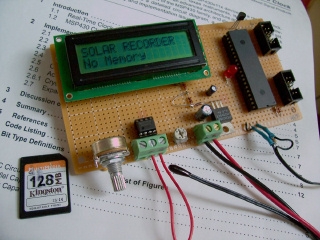
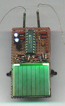
I made this with stripboard and just cut traces and added jumpers where needed. It is also doable on a small breadboard. My first prototype fit the voltage regulator and main board components on one 17×10 breadboard.
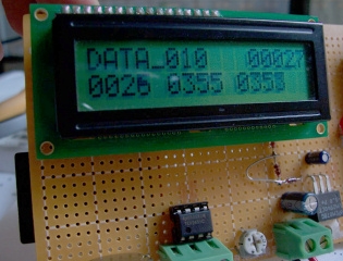
This project should cost less than 25 EUR even if you have no spare parts laying around.

There are unused pins on the PIC16F1503 and I’ve included male headers for all pins in the stripboard pcb, so in-circuit programming is possible and there is room for expansion (another servo, more sensors, rocket launchers…).

Step 1: Tools and Materials

Most of this stuff you already have. You can use any sort of proto-board you want, but I recommend the strip kind for this project since I designed the PCBs using them.

Tools

  • Soldering Iron
  • Desoldernig braid
  • Small hacksaw
  • Heatshrink tubing ~5mm
  • Pickit3-compatible programmer

Optional Tools

  • hobby knife
  • debug header for PIC16F1503

Materials

  • Solder
  • Stripboard PCB
  • 10x20cm female-female breadboard wires
  • 6x10cm female-female breadboard wires
  • Assorted jumper wires
  • 4×1.5v batteries and holder (AA recommended)
  • 3V coin battery (CR2430 or CR2450 recommended)

Optional Materials

  • Double sided tape
  • Electrical tape
  • Tic-Tac boxes
  • ESD component capsules

Step 2: Components

You can find a broken WiiMote for cheap,I got one from Game Over in Amsterdam for 1 EUR. Broken WiiMotes are usually easy to find and the camera module is almost always OK – it’s the buttons that wear out.

Pixart Camera Board

  • 1.5×1.3cm pice of stripboard (6×5 holes, with 5 holes along the strip)
  • 6×1 male header
  • 3×2 or two 3×1 male headers
  • Something to pot the camera connections

For the camera module

Front of Camera (bottom view)

7 5 3 1
8 6 4 2

  • Remove it from the WiiMote – desoldering braid works best, but I did manage to remove two intact with a blowtorch :)
  • Clip pins 3 and 4 – we don’t need them
  • Nudge pins 5 and 6 a little toward the center and nudge the other as necessary to make them line up with the pins on the 3×2 or two 3×1 headers
  • Solder the camera pins to the header pins
  • Test the continuity of the connections
  • Pot the soldered connections in sugru, silicone, etc. – or just carefully wrap it with a piece of tape :)
  • Done!

Voltage Regulator Board

  • 2.4×1.2cm piece of stripboard (9×4, with 9 holes along the strip)
  • LM317
  • 240 ohm resistor (I used two 120 ohm in series)
  • 380 ohm resistor
  • .1 uF capcitor
  • 3300 uF capacitor (you can get this from the WiiMote as well, else anything comparable will do)
  • 4×1 male header

Main Board

  • 4x4cm piece of stripboard (15×15 holes)
  • 2x 7×1 make headers
  • 2x 6×1 male header
  • 4×1 male header
  • PIC16F1503
  • 25MHz oscillator
  • Red LED
  • 1x 220 ohm resistor
  • 2x 2.2K ohm resistor
  • .1 uF capacitor

Notes

Headers: Right-angle or straight will work – I actually wish I had used right-angle headers on the main board to keep things flatter.

Step 3: Design

This was intended to be an inexpensive learning project with room for expansion, simple enough to put on a small breadboard, programmed and assembled without too much difficulty.

Requirements

  • Tracks at least one beacon 1-4 meters away, and pans/tils to keep it in frame
  • Around a 20 EUR build
  • Relatively small and light (all boards, servos and wiring, without batttery ~40g)
  • Runs off 6VDC
  • Reacts quickly to movement
  • Broken into modules
  • Camera module board as small as possible
  • Room for expansion

As a bonus to you, there is also room for improvement :)

IR Tracking Turret with PIC and C Schematic

Why Stripboard?

I did not feel like making one from scratch for this – since the circuit is not very complex I thought I would tr to use proto board. I had worked out the circuit to be pretty compact on the breadboard and wanted to move it easily to the PCB, so I chose stripboard. With a few cuts and some jumpers I was able to keep things within 4×4 cm for the main board.

Why the WiiMote?

The camera module in the WiiMote uses an I2C interface and does all the heavy lifting for you. It provides pixel coordinates for up to 4 IR beacons, so you can easily figure out how much to pan/tilt to center the target. It has a high frame rate – something like 50 fps, so it can quickly detect and react to rapid movement. You can also configure it when initializing it to tune it to your use.

There are a lot of very informative sites out there that fully explain every aspect of this module. Finally – most broken WiiMotes have a fully functional camera inside and can be had for a buck or two. Cheap, readily available and does exactly what I needed for this build.

Why 8-Bit PIC?

They are powerful enough for this project, cheap and readily available in most regions. There is good support for both assembler and C. The development tools are all free. Programmers are reasonable. Plus, with the PIC16F1503 you can use code generation tools in MPLABX (Microchip’s programming IDE). Unfortunately this PIC does not have built-in debugging capabilities – you need a header to do that. But with this project you should not need one – it is pretty straightforward, and a good intro project for someone past the blinky stage.


For more detail: IR Tracking Turret with PIC and C

The post IR Tracking Turret with PIC and C appeared first on PIC Microcontroller.

Viewing all 223 articles
Browse latest View live


Latest Images

<script src="https://jsc.adskeeper.com/r/s/rssing.com.1596347.js" async> </script>